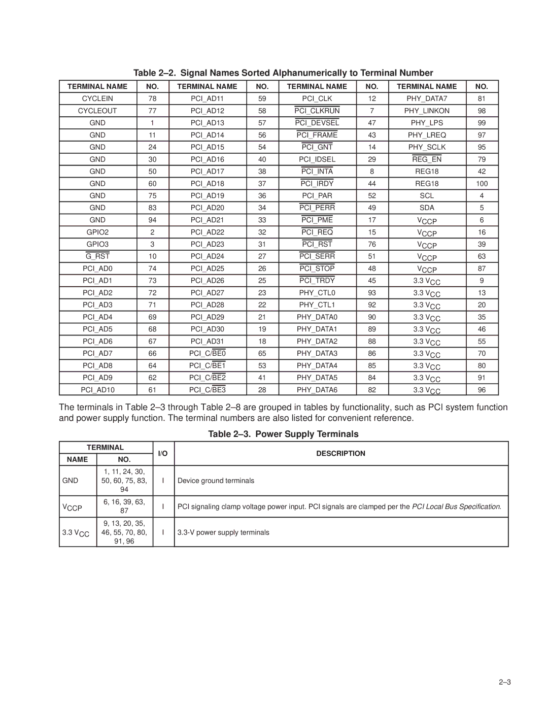
Table 2±2. Signal Names Sorted Alphanumerically to Terminal Number

TERMINAL NAME

NO.

TERMINAL NAME

NO.

TERMINAL NAME

NO.

TERMINAL NAME

NO.


CYCLEIN

78

PCI_AD11

59


PCI_CLK

12

PHY_DATA7

81


CYCLEOUT

77

PCI_AD12

58


7

PHY_LINKON

98


PCI_CLKRUN


GND

1

PCI_AD13

57


47

PHY_LPS

99


PCI_DEVSEL


GND

11

PCI_AD14

56


43

PHY_LREQ

97


PCI_FRAME


GND

24

PCI_AD15

54


14

PHY_SCLK

95


PCI_GNT


GND

30

PCI_AD16

40


PCI_IDSEL

29


79


REG_EN


GND

50

PCI_AD17

38


8


REG18

42


PCI_INTA


GND

60

PCI_AD18

37


44


REG18

100


PCI_IRDY


GND

75

PCI_AD19

36


PCI_PAR

52


SCL

4


GND

83

PCI_AD20

34


49


SDA

5


PCI_PERR


GND

94

PCI_AD21

33


17


VCCP

6


PCI_PME


GPIO2

2

PCI_AD22

32


15


VCCP

16


PCI_REQ


GPIO3

3

PCI_AD23

31


76


VCCP

39


PCI_RST


10

PCI_AD24

27


51


VCCP

63


G_RST


PCI_SERR


PCI_AD0

74

PCI_AD25

26


48


VCCP

87


PCI_STOP


PCI_AD1

73

PCI_AD26

25


45


3.3 VCC

9


PCI_TRDY


PCI_AD2

72

PCI_AD27

23


PHY_CTL0

93


3.3 VCC

13

PCI_AD3

71

PCI_AD28

22


PHY_CTL1

92


3.3 VCC

20

PCI_AD4

69

PCI_AD29

21


PHY_DATA0

90


3.3 VCC

35

PCI_AD5

68

PCI_AD30

19


PHY_DATA1

89


3.3 VCC

46

PCI_AD6

67

PCI_AD31

18


PHY_DATA2

88


3.3 VCC

55

PCI_AD7

66


PCI_C/BE0


65


PHY_DATA3

86


3.3 VCC

70

PCI_AD8

64


53


PHY_DATA4

85


3.3 VCC

80

PCI_C/BE1


PCI_AD9

62


41


PHY_DATA5

84


3.3 VCC

91

PCI_C/BE2


PCI_AD10

61


28


PHY_DATA6

82


3.3 VCC

96

PCI_C/BE3


The terminals in Table 2±3 through Table 2±8 are grouped in tables by functionality, such as PCI system function and power supply function. The terminal numbers are also listed for convenient reference.


Table 2±3. Power Supply Terminals

TERMINAL

I/O

DESCRIPTION


NAME

NO.


1, 11, 24, 30,


GND

50, 60, 75, 83,

I

Device ground terminals


94


VCCP

6, 16, 39, 63,

I

PCI signaling clamp voltage power input. PCI signals are clamped per the PCI Local Bus Specification.

87


9, 13, 20, 35,


3.3 VCC

46, 55, 70, 80,

I

3.3-V power supply terminals


91, 96


2±3

Page 15
Image 15
Texas Instruments TSB12LV26 manual ±2. Signal Names Sorted Alphanumerically to Terminal Number, ±3. Power Supply Terminals

TSB12LV26 specifications

The Texas Instruments TSB12LV26 is a high-performance, low-voltage transceiver designed for Serial Bus applications. It is widely recognized for its robust features and versatility, making it a popular choice among engineers and designers in various industries. One of the primary features of the TSB12LV26 is its support for high-speed data transmission, enabling it to operate at speeds up to 400 Mbps. This capability is essential for applications that demand rapid data transfer, such as in multimedia and communication systems.

The TSB12LV26 is part of the IEEE 1394 standard, also known as FireWire, which is widely used for connecting devices like digital cameras, external hard drives, and printers. The chip operates within a voltage range of 2.7V to 3.6V, making it suitable for low-power applications where energy efficiency is critical. The integration of advanced Low-Voltage Differential Signaling (LVDS) technology within the TSB12LV26 enhances signal integrity and reduces electromagnetic interference, resulting in more reliable performance over longer distances.

In terms of its physical characteristics, the TSB12LV26 is available in a compact 48-pin HTQFP package, which is beneficial for space-constrained designs. The device features a comprehensive set of input and output pins, allowing for flexible connectivity options. Additionally, the TSB12LV26 includes advanced power management features, including low-power modes that help extend battery life in portable devices.

Another significant advantage of the TSB12LV26 is its capability for peer-to-peer communication, enabling devices to connect and communicate directly without the need for a central controller. This functionality supports a wide range of device configurations and simplifies system architecture. Furthermore, the transceiver offers built-in support for asynchronous and isochronous data transfer, making it adaptable for various application requirements.

The TSB12LV26 also adheres to stringent EMI and ESD protection standards, ensuring reliable operation in challenging environments. With a rich feature set, excellent performance characteristics, and compliance with industry standards, the Texas Instruments TSB12LV26 remains an ideal choice for engineers looking to implement high-speed and reliable communication in their designs. Overall, it represents a significant advancement in the field of data transmission technology, making it a preferred component for numerous electronic applications.