HARDWARE-CIRCUITS OR ANY OTHER KIND OF ASIC OR PROGRAMMABLE LOGIC DESIGN), EVEN IF THE COPYRIGHT HOLDER HAS BEEN ADVISED OF THE POSSIBILITY OF SUCH DAMAGES.
Design “usbs6_soc”
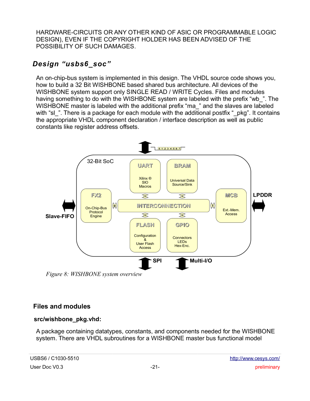
An on-chip-bus system is implemented in this design. The VHDL source code shows you, how to build a 32 Bit WISHBONE based shared bus architecture. All devices of the WISHBONE system support only SINGLE READ / WRITE Cycles. Files and modules having something to do with the WISHBONE system are labeled with the prefix “wb_”. The WISHBONE master is labeled with the additional prefix “ma_” and the slaves are labeled with “sl_”. There is a package for each module with the additional postfix “_pkg”. It contains the appropriate VHDL component declaration / interface description as well as public constants like register address offsets.
0 1 2 3 4 5 6 7 
UART BRAM
| | | Xilinx ® | Universal Data | | | |
| | | SIO | | | |
| | | Source/Sink | | | |
| | | Macros | | | |
| | | | | | |
| FX2 | | S | S | | MCB | LPDDR |
| On-Chip-Bus | M | INTERCONNECTION | S | | |
| | | | | |
| Protocol | | | | | Ext.-Mem. | |
Slave-FIFO | | S | S | | Access | |
Engine | | | |
| | | | | |
| | | FLASH | GPIO | | | |
| | | Configuration | Connectors | | | |
| | | & | | | |
| | | LEDs | | | |
| | | User Flash | | | |
| | | Hex-Enc. | | | |
| | | Access | | | |
| | | | | | |
| | | SPI | Multi-I/O | | |
Figure 8: WISHBONE system overview | | | | |
Files and modules
src/wishbone_pkg.vhd:
A package containing datatypes, constants, and components needed for the WISHBONE system. There are VHDL subroutines for a WISHBONE master bus functional model
USBS6 / C1030-5510 | | http://www.cesys.com/ |
User Doc V0.3 | -21- | preliminary |

![]()
