src/sync_fifo.vhd:
This entity is a general purpose synchronous FIFO buffer. It is build of FPGA distributed RAM.
src/sfifo_hd_a1Kx18b0K5x36.vhd:
This entity is a general purpose synchronous FIFO buffer with mismatched port widths. It is build of a FPGA BlockRAM.
src/flash_ctrl.vhd:
The low level FLASH controller for SPI FLASH memory. It supports reading and writing of four bytes of data at one time as well as erasing the whole memory.
usbs6_soc.xise:
Project file for XilinxTM ISE
usbs6_soc.ucf:
User constraint file with timing and pinout constraints
usbs6_soc_fpga_consts.h:
C header file extracted from VHDL packages. It contains address, flag, bitfield and value definitions for FPGA design access integration into host software application.
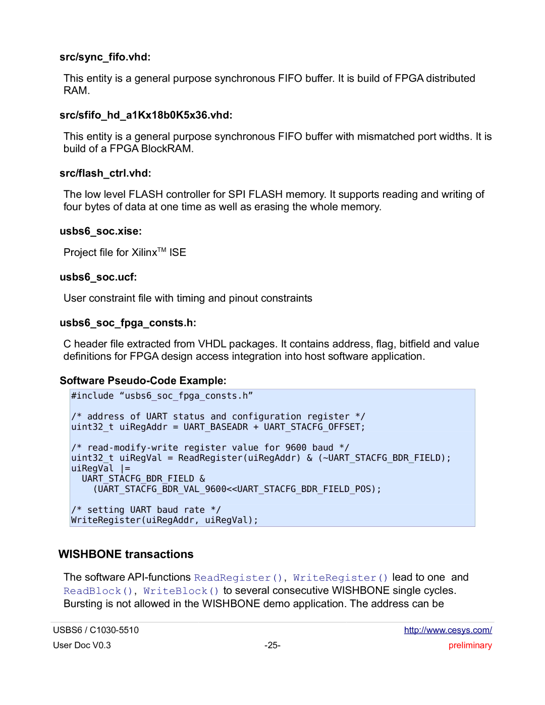
Software Pseudo-Code Example:
#include “usbs6_soc_fpga_consts.h”
/* address of UART status and configuration register */ uint32_t uiRegAddr = UART_BASEADR + UART_STACFG_OFFSET;
/*
uint32_t uiRegVal = ReadRegister(uiRegAddr) & (~UART_STACFG_BDR_FIELD); uiRegVal =
UART_STACFG_BDR_FIELD & (UART_STACFG_BDR_VAL_9600<<UART_STACFG_BDR_FIELD_POS);
/* setting UART baud rate */ WriteRegister(uiRegAddr, uiRegVal);
WISHBONE transactions
The software
USBS6 / |
| http://www.cesys.com/ |
User Doc V0.3 | preliminary |