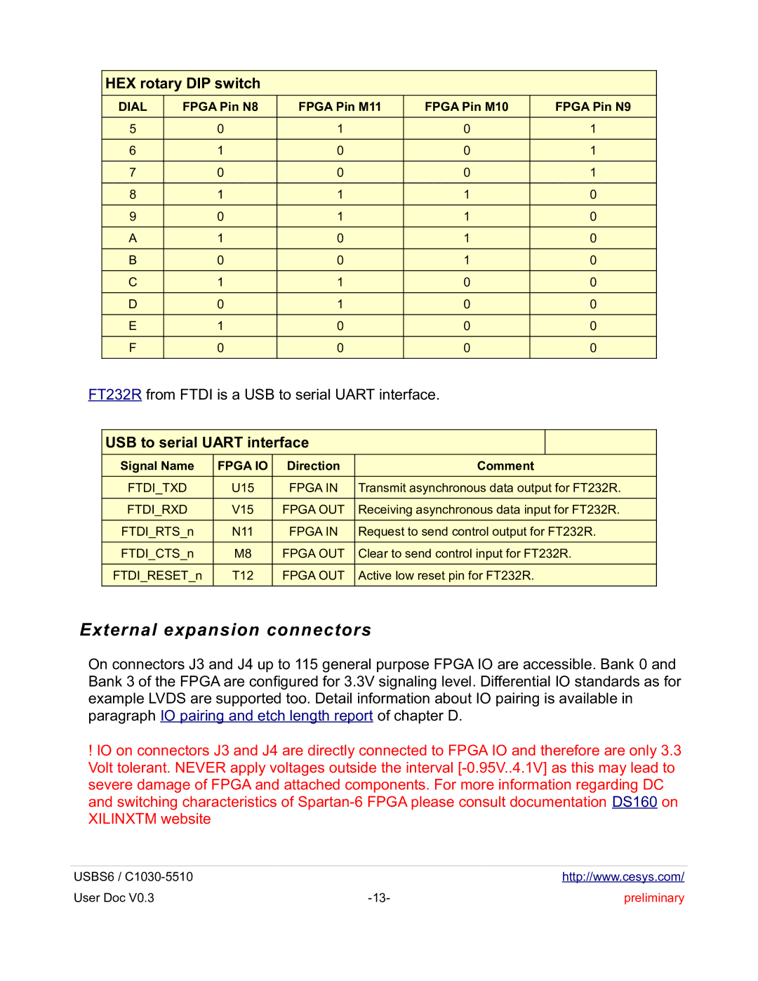
 HEX rotary DIP switch
DIAL | FPGA Pin N8 | FPGA Pin M11 | FPGA Pin M10 | FPGA Pin N9 |
|
|
|
|
|
5 | 0 | 1 | 0 | 1 |
6 | 1 | 0 | 0 | 1 |
7 | 0 | 0 | 0 | 1 |
8 | 1 | 1 | 1 | 0 |
9 | 0 | 1 | 1 | 0 |
A | 1 | 0 | 1 | 0 |
B | 0 | 0 | 1 | 0 |
C | 1 | 1 | 0 | 0 |
D | 0 | 1 | 0 | 0 |
E | 1 | 0 | 0 | 0 |
F | 0 | 0 | 0 | 0 |
|
|
|
|
|
FT232R from FTDI is a USB to serial UART interface.
 USB to serial UART interface
Signal Name | FPGA IO | Direction | Comment |
FTDI_TXD | U15 | FPGA IN | Transmit asynchronous data output for FT232R. |
FTDI_RXD | V15 | FPGA OUT | Receiving asynchronous data input for FT232R. |
FTDI_RTS_n | N11 | FPGA IN | Request to send control output for FT232R. |
FTDI_CTS_n | M8 | FPGA OUT | Clear to send control input for FT232R. |
FTDI_RESET_n | T12 | FPGA OUT | Active low reset pin for FT232R. |
|
|
|
|
External expansion connectors
On connectors J3 and J4 up to 115 general purpose FPGA IO are accessible. Bank 0 and Bank 3 of the FPGA are configured for 3.3V signaling level. Differential IO standards as for example LVDS are supported too. Detail information about IO pairing is available in paragraph IO pairing and etch length report of chapter D.
!IO on connectors J3 and J4 are directly connected to FPGA IO and therefore are only 3.3 Volt tolerant. NEVER apply voltages outside the interval
USBS6 / |
| http://www.cesys.com/ |
User Doc V0.3 | preliminary |
