|
|
| Basic WISHBONE cycle | |
CLK |
|
|
| |
STB |
|
| ||
WE |
|
| Master | |
ADR32 | ||||
| ||||
DAT |
| M |
| |
DAT | 32 |
| ||
| S | Slave | ||
| 32 | |||
ACK |
|
| ||
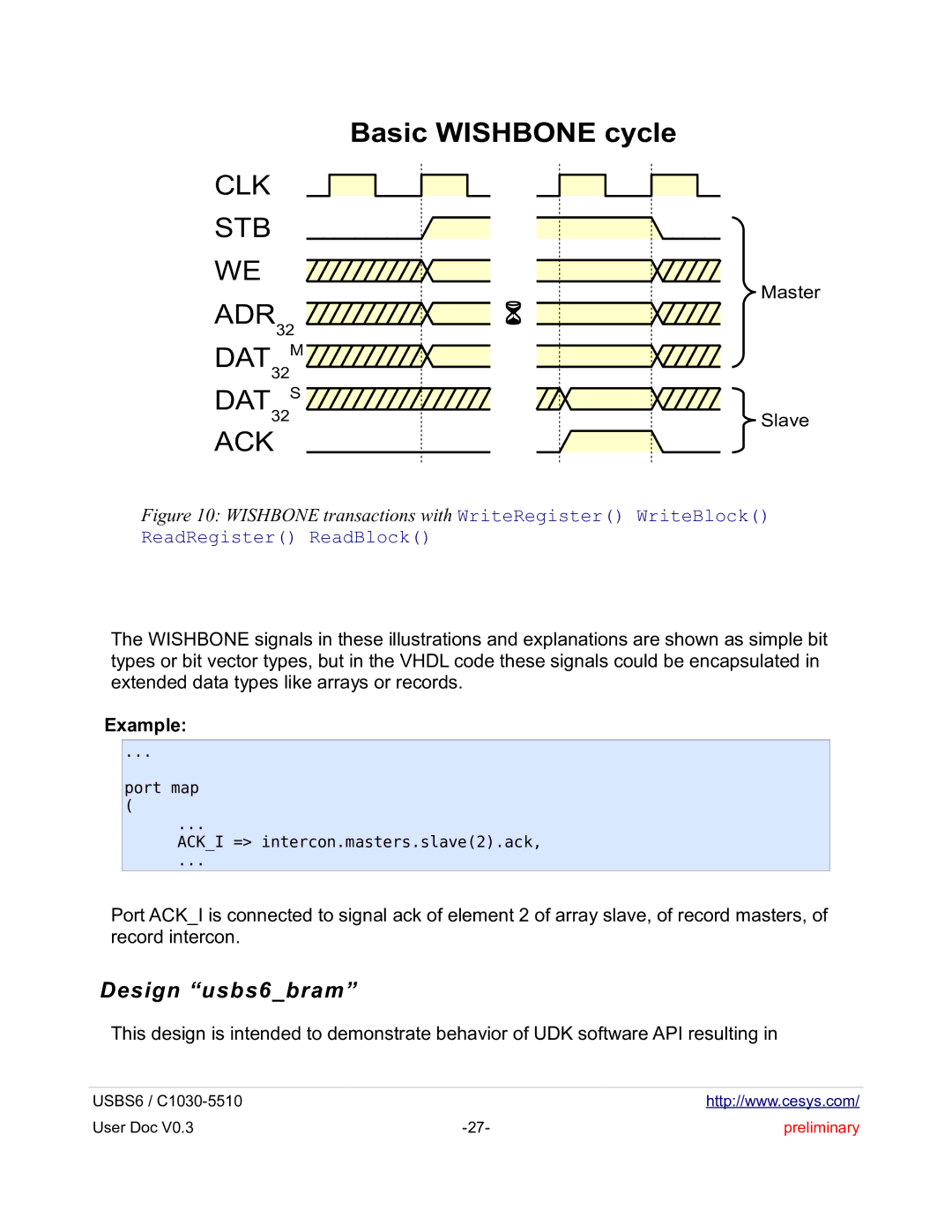
Figure 10: WISHBONE transactions with WriteRegister() WriteBlock()
ReadRegister() ReadBlock()
The WISHBONE signals in these illustrations and explanations are shown as simple bit types or bit vector types, but in the VHDL code these signals could be encapsulated in extended data types like arrays or records.
Example:
...
port map
(
...
ACK_I => intercon.masters.slave(2).ack,
...
Port ACK_I is connected to signal ack of element 2 of array slave, of record masters, of record intercon.
Design “usbs6_bram”
This design is intended to demonstrate behavior of UDK software API resulting in
USBS6 / |
| http://www.cesys.com/ |
User Doc V0.3 | preliminary |
