 LPDDR SDRAM
 MT46H64M16LFCK-5
Signal Name | FPGA IO | Comment |
MCB1_DQ12 | T17 |
|
MCB1_DQ13 | T18 |
|
MCB1_DQ14 | U17 |
|
MCB1_DQ15 | U18 |
|
MCB1_UDQS | N15 | Data strobe for Upper Byte Data bus: Output with read data, input |
|
| with write data. DQS is |
|
| write data. It is used to capture data. |
*As the memory device interface of
!It is strongly recommended to check XILINXTM user guide UG388 about
!It is strongly recommended to check XILINXTM user guide UG416 about
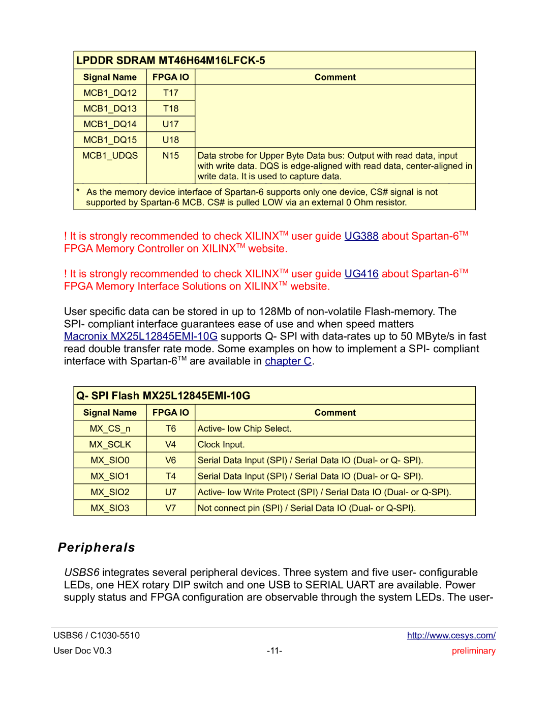
User specific data can be stored in up to 128Mb of
Macronix
 Q- SPI Flash
 MX25L12845EMI-10G
Signal Name | FPGA IO | Comment |
|
|
|
MX_CS_n | T6 | Active- low Chip Select. |
MX_SCLK | V4 | Clock Input. |
MX_SIO0 | V6 | Serial Data Input (SPI) / Serial Data IO (Dual- or Q- SPI). |
MX_SIO1 | T4 | Serial Data Input (SPI) / Serial Data IO (Dual- or Q- SPI). |
MX_SIO2 | U7 | Active- low Write Protect (SPI) / Serial Data IO (Dual- or |
MX_SIO3 | V7 | Not connect pin (SPI) / Serial Data IO (Dual- or |
|
|
|
Peripherals
USBS6 integrates several peripheral devices. Three system and five user- configurable LEDs, one HEX rotary DIP switch and one USB to SERIAL UART are available. Power supply status and FPGA configuration are observable through the system LEDs. The user-
USBS6 / |
| http://www.cesys.com/ |
User Doc V0.3 | preliminary |
