User Manual January Supersedes September
LCX9000 Liquid-Cooled Drives
MN04005001E
Page
Important Notice - Please Read
Table of
CHAPTER 4 - CONTROL WIRING AND INTERNAL CONNECTIONS
Contents
List of Figures
List of Figures Continued
List of Tables
Table 5-13 Resettable Counters
List of Tables Continued
Table A-1 Fault Codes
Table 5-11 System Menu Functions
Definitions and Symbols
Safety
Hazardous High Voltage
Warnings
Warnings, Cautions and Notices
Cautions
Motor and Equipment Safety
Grounding and Ground Fault Protection
Receiving and Inspection
Chapter 1 - Overview
L C X 0 1 6 A 0 - 4 A 2 B
Technical Data
Maintenance
Storage and Shipping
LCX9000 Liquid-Cooled Drives User Manual
Figure 1-1 Liquid-Cooled Drive Principal Block Diagram
Drives
Power Ratings
Page
Page
Table 1-4 Technical Information
Specifications
1-10
Table 1-4 Technical Information Continued
Mounting
Chapter 2 - Installation
Lifting the Drive
Table 2-1 One-Module Drive Dimensions Mounting Base Included
Liquid-Cooled Dimensions
Drives Consisting of One Module
Figure 2-2 LCX9000 Liquid-Cooled Drive, CH3
Figure 2-4 LCX9000 Liquid-Cooled Drive, CH5
Figure 2-3 LCX9000 Liquid-Cooled Drive, CH4
Bottom View
Top View
Figure 2-6 LCX9000 Liquid-Cooled Drive, CH72
Figure 2-5 LCX9000 Liquid-Cooled Drive, CH61
Drives Consisting of Several Modules
Table 2-2 Several Module Drive Dimensions Mounting Bracket Included
Figure 2-7 Drive Mounted Inside Mounting Bracket
Figure 2-8 LCX9000 Liquid-Cooled Drive with Mounting Bracket, CH63
Bottom
Figure 2-9 LCX9000 Liquid-Cooled Drive, CH74, IP00
6-Pulse Supply
12-Pulse Supply
Drinking Water Specification
Cooling
Table 2-3 Drinking Water Chemical Specification
Table 2-4 Drinking Water Quality Recommendations - Maximum Values
Table 2-6 Process Water Specification
Table 2-5 Drinking Water Quality Recommendations - Desired Values
Exchanger
Figure 2-10 Example of Cooling System
Heat
Table 2-7 Information About Cooling Agent and Its Circulation
Figure 2-11 Example PI-Diagram of Cooling System and Connections
Table 2-9 Coolant Volumes and Temperatures
Figure 2-12 Safe Operating Conditions in Relation to Condensation
Condensation
Cooling System Connections
Table 2-10 Liquid Connector Types All Pressure Values at Nominal Flow
Figure 2-13 Aluminum Hose Adapters
Figure 2-14 External Thread of Hose
Figure 2-15 Pressure Loss - CH6x
Pressure Losses Table 2-11 Pressure Losses - CH6x
Outflow Hoses and
Figure 2-16 Pressure Loss - CH7x
Table 2-12 Pressure Losses - CH7x
The following main line hose materials are acceptable plastic PVC
rubber EPDM only aluminium other stainless and acid-proof materials
About Flow Switch Installation
Installation of Flow Switch
Figure 2-17 Flow Switch Hose Connection, Fast Connector Electrical
Fast Connector Lock Screw, Cable Seal and Clamp
External Cooling Fan for CH4
Figure 2-18 Direction of Coolant Circulation
Drive Derating
Input Chokes
Table 2-16 Input Choke Dimensioning, 6-Pulse Supply
Figure 2-19 Example of Input Chokes for Liquid-Cooled Sizes Up to 62A
Installation of Input Choke
Figure 2-20 Example of Input Chokes for Liquid-Cooled
Sizes 87 - 145A and 590A
January
Table 2-17 Choke Dimensions Sizes 23 - 145A and 590A
Table 2-18 Choke Dimensions Sizes 261 - 1150A
LCX9000 Liquid-Cooled Drives User Manual
Power Connections
Chapter 3 - Power Wiring
Mains Cable
Motor Cable
Cable Data
Table 3-1 Cable Types Required to Meet Standards
Table 3-2 Cable Sizes 400
Units with 6-pulse supply
Table 3-2 Cable Sizes 400 - 500V Continued
Units with 12-pulse supply
Three grounding terminals per mounting plate, see Page
Table 3-4 Tightening Torques of Bolts
Table 3-3 Cable Sizes 525
See the tightening torques of bolts in Table
Table 3-5 Fuse Sizes for LCX9000 Liquid-Cooled 500V Drives
Fuse Sizes, Drives
Fuse information
Table 3-6 Fuse Sizes for LCX9000 Liquid-Cooled 690V Drives
The maximum length of the motor cables is 984 feet 300m
Cable Installation Instructions
4. If cable insulation checks are needed, see Page
Figure 3-1 Maximum Terminal Stresses
Figure 3-2 Installation Space
Installation Space
Cable Installation and the UL Standards
Grounding of Power Unit
Figure 3-3 Grounding Terminal on Mounting Plate
Cable and Motor Insulation Checks
3-12
Figure 4-1 Control Board
Chapter 4 - Control Wiring and Internal Connections
Figure 4-3 Drives Connected in Parallel
Figure 4-2 Basic and Option Board Connections of the Control Board
Figure 4-4 Connection of Control Board Cable from the Power Board
Control Board Power-Up
See Figures 4-4 and
WRONG Terminal J1 Upper
Control Connections
Figure 4-5 Connection of Control Board Cable from the Power Board
CORRECT Terminal J2 Lower
Figure 4-6 I/O Terminals of the Two Basic Boards
Figure 4-8 General Wiring Diagram of the Basic Relay Board OPT-A2
Figure 4-7 General Wiring Diagram of the Basic I/O Board OPT-A9
Galvanic Isolation Barriers
Control Cables
Figure 4-9 Galvanic Isolation Barriers
Table 4-1 Control I/O Terminal Signals
Control Terminal Signals
Figure 4-10 Positive/Negative Logic
Digital Input Signal Inversions
Jumper Selections on the OPT-A9 Basic Board
Figure 4-11 Jumper Blocks on OPT-A9
AI1 Mode
Figure 4-12 Jumper Selection for OPT-A9
AI2 Mode
AO1 Mode
Figure 4-14 Control Unit Installed into the Mounting Box
Installing the Control Unit Mounting Box
Control Unit Mounting Box
Figure 4-13 Control Unit Mounting Box
Table 4-2 Installing the Control Unit Mounting Box
January MN04005001E
Table 4-2 Installing the Control Unit Mounting Box Continued
Internal Connections
Connections between Power Unit ASIC and Driver Boards
CH61, CH62 and CH72 Table 4-3 Terminals CH61, CH62 and CH72
Figure 4-15 Terminals and Connections between ASIC and Driver Board
X9 OEVA feedback X15 Charging relay output X6 DC terminal
X29 Flow supervision input
Connect to WL on Phase V/W driver board
Table 4-4 Terminals CH63
Table 4-5 Terminals between Driver Boards CH64 and CH74
Figure 4-18 Remove Cover to Access Power Unit
Connections between Power Unit ASIC and the Control Unit
Connections with Round Cable
Connections with Optical Cable
Table 4-6 Terminals on Adapter Board
Figure 4-19 Optical Cable Adapter Board
Supply voltage 24Vin from power unit
Control board connection
Chapter 5 - Menu Information
Indicators on the Keypad Display
Keypad Operation
Figure 5-1 Control Keypad and Drive Status Indications
Table 5-1 Drive Status Indicators
Drive Status Indicators
Control Place Indicators
Table 5-2 Control Place Indicators
Status LEDs Green - Green - Red
Keypad Pushbuttons
Table 5-3 Status LEDs Green - Green - Red
Text Lines
Table 5-5 Button Descriptions
Figure 5-3 Keypad Display Data
Menu Navigation
Monitor
Figure 5-4 Keypad Navigation Chart
Figure 5-5 Monitoring Menu
Monitoring Menu M1
Parameter Menu M2
Table 5-6 Monitored Signals
Keypad Control Menu M3
Figure 5-6 Parameter Value Change Procedure
Table 5-7 Keypad Control Parameters, M3
Figure 5-7 Selection of Control Place Keypad Reference
Selection of Control Place
Keypad Direction
Figure 5-8 Normal State, No Faults
Active Faults Menu M4
STOP Button Activated
Figure 5-9 Fault Display Table 5-8 Fault Types
Fault Types
Fault Time Data Record
Fault Type Symbol
Fault History Menu M5
Table 5-9 Fault Time Recorded Data
Real Time Record
Table 5-10 Real Time Record
System Menu M6
Figure 5-10 Fault History Menu
Table 5-11 System Menu Functions
5-16
Table 5-11 System Menu Functions Continued
Figure 5-11 Selection of Language Application Selection
Selection of Language
Figure 5-12 Change of Application
Parameter Sets S6.3.1
Copy Parameters
Figure 5-13 Storing and Loading of Parameter Sets
Upload parameters to keypad To keypad, S6.3.2
Figure 5-14 Parameter Copy to Keypad
Automatic Parameter Backup P6.3.4
Download parameters to drive From keypad, S6.3.3
Figure 5-15 Parameter Comparison
Parameter Comparison
P2.1.2= 20.0 Hz
Figure 5-16 Password Setting
Password S6.5.1
Security
Figure 5-17 Parameter Locking
Parameter Lock P6.5.2
Start-Up Wizard P6.5.3
Figure 5-18 Activation of Start-Up Wizard
Figure 5-20 Keypad Settings Submenu
Keypad Settings
Default Page P6.6.1
Figure 5-21 Default Page Function
Timeout Time P6.6.3
Default page in the operating menu P6.6.2
Figure 5-22 Timeout Time Setting
Contrast Adjustment P6.6.4
HMI Acknowledge Timeout P6.7.3
Hardware Settings
Figure 5-23 HMI Acknowledge Timeout
System info
Number of retries to receive HMI acknowledgement P6.7.4
Total Counters
Table 5-12 Counter Pages
Figure 5-24 Counter Reset
Table 5-13 Resettable Counters
Trip Counters
Software S6.8.3
Table 5-15 Applications Information Pages
Applications S6.8.4
Figure 5-25 Applications Info Submenu
Hardware S6.8.5
Figure 5-26 Expander Board Information Menus
Expander Boards S6.8.6
Debug Menu S6.8.7
Expander Board Menu M7
Expander Board Parameters
Further Keypad Functions
Table 5-17 Expander Board Parameters Board OPTA1
Figure 5-27 Expander Board Information Menu
Chapter 6 - Start-Up
Safety Precautions
Sequence of Operation
Page
January
Table A-1 Fault Codes
Appendix A - Fault Codes
Table A-1 Fault Codes Continued
Table A-1 Fault Codes Continued
Load Test with Motor
DC Link Test without Motor
January
Figure B-1 Main Circuit and Control Diagram, CH3
Main Circuit and Control Diagrams
Appendix B - Technical Reference
Figure B-3 Main Circuit and Control Diagram, CH5
Figure B-2 Main Circuit and Control Diagram, CH4
Term
ATerm
Figure B-5 Main Circuit and Control Diagram, CH61, Control
Figure B-4 Main Circuit and Control Diagram, CH61
SPF1
H8...H13
Figure B-7 Main Circuit and Control Diagram, CH63, Module
Figure B-6 Main Circuit and Control Diagram, CH63, Module
VB00491
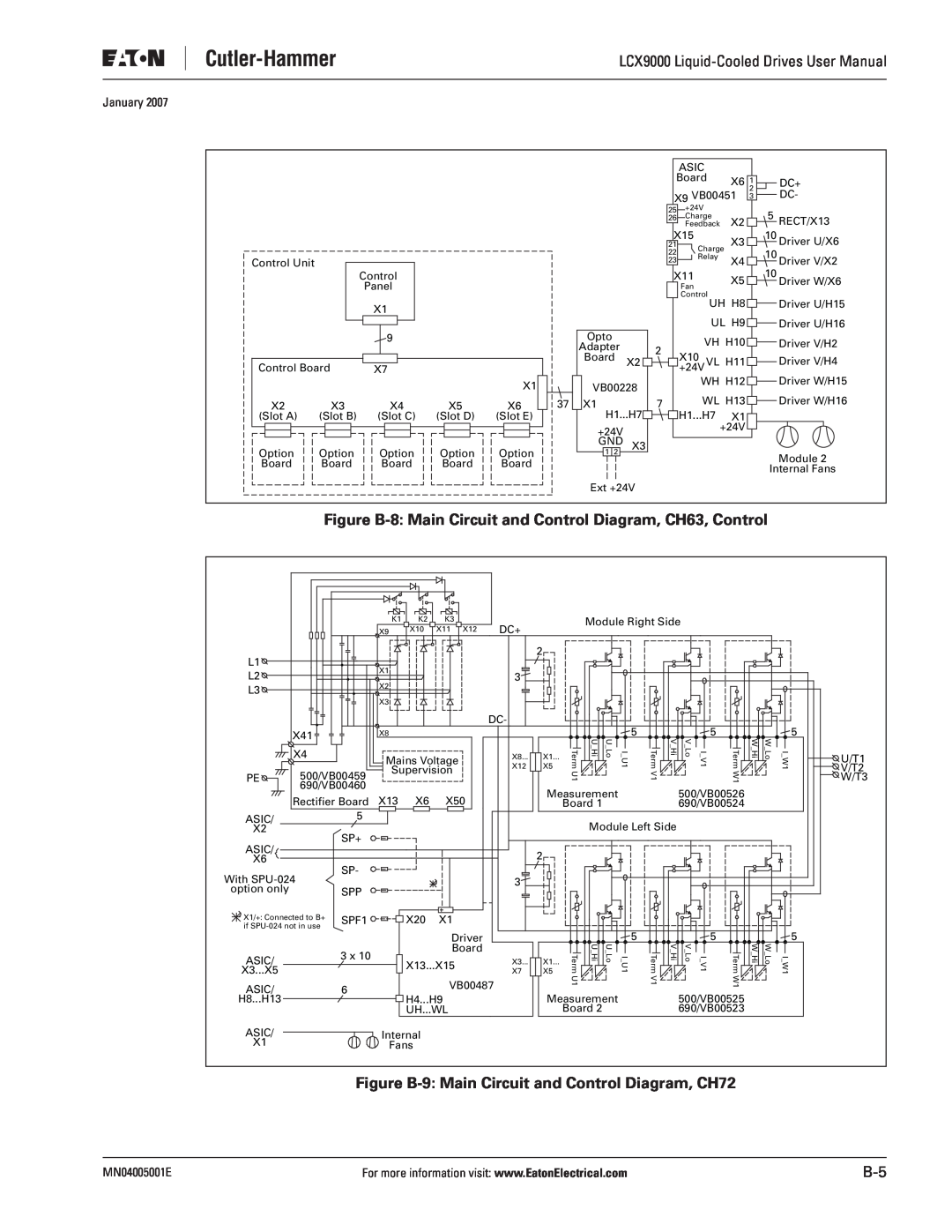
Figure B-9 Main Circuit and Control Diagram, CH72
Figure B-8 Main Circuit and Control Diagram, CH63, Control
Figure B-11 Main Circuit and Control Diagram, CH74, Phase U
Figure B-10 Main Circuit and Control Diagram, CH72, Control
Figure B-12 Main Circuit and Control Diagram, CH74, Control
Figure B-13 Fan Mounting Pallet - Hot Dip Zinc Coated
Fan Dimensions
Figure B-14 Fan Support
January
B-10
Page
Eaton Electrical Inc
Company Information
2007 Eaton Corporation All Rights Reserved Printed in USA
Publication No. MN04005001E/CPG January