2 |
Hardware Preparation and Installation
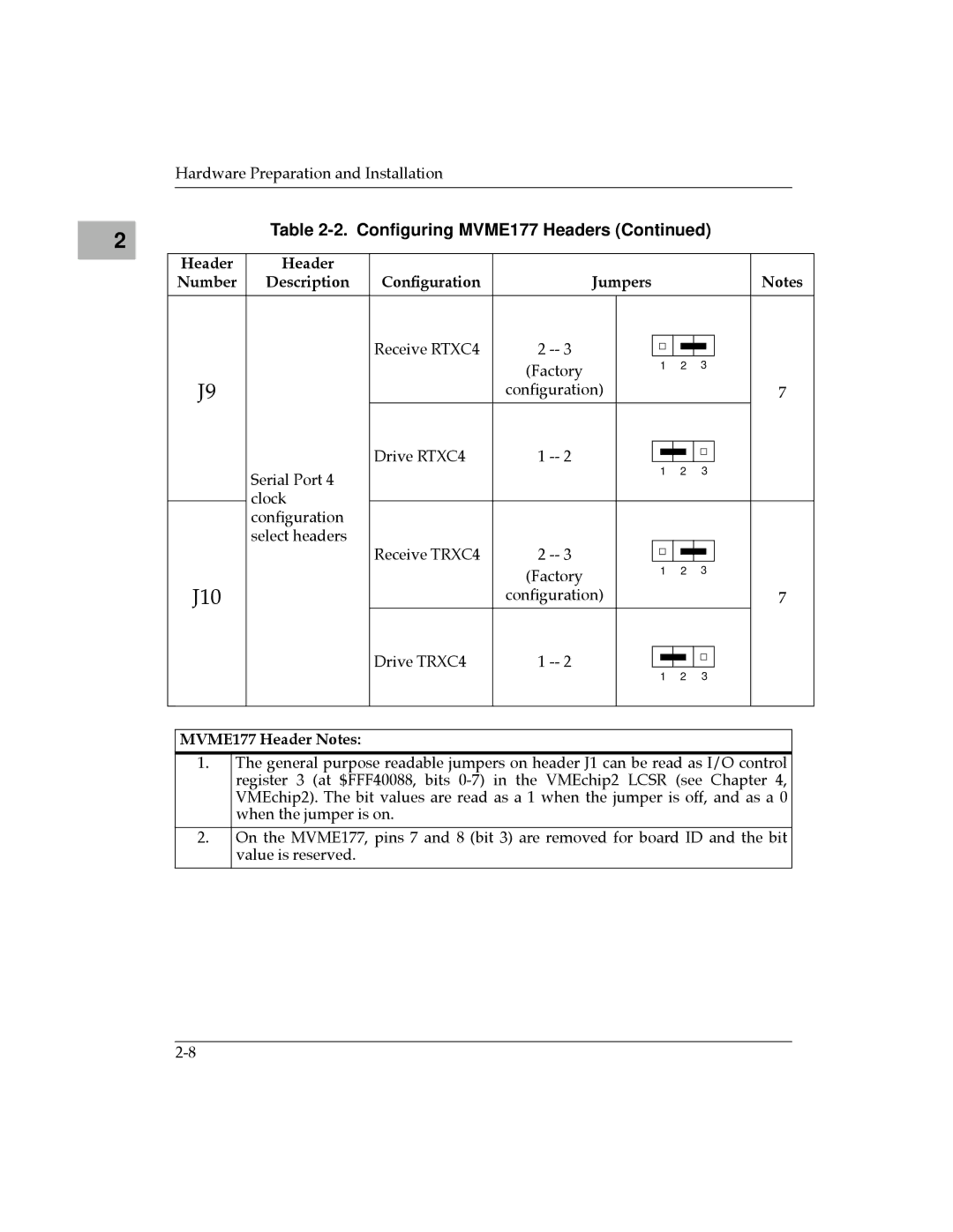
Table 2-2. Configuring MVME177 Headers (Continued)
Header | Header |
|
|
|
|
|
|
|
|
|
|
|
|
Number | Description | ConÞguration | Jumpers |
|
|
|
|
|
|
|
| Notes | |
|
|
|
|
|
|
|
|
|
|
|
|
|
|
|
| Receive RTXC4 | 2 |
|
|
|
|
|
|
|
|
|
|
|
|
|
|
|
|
|
|
|
|
|
| ||
|
|
|
|
|
|
|
|
|
|
|
| ||
|
|
|
|
|
|
|
|
|
|
|
| ||
|
|
| (Factory |
| 1 | 2 | 3 |
|
| ||||
J9 |
|
|
|
|
|
|
|
|
|
|
|
| |
|
| conÞguration) |
|
|
|
|
|
|
|
|
| 7 | |
|
| Drive RTXC4 | 1 |
|
|
|
|
|
|
|
|
|
|
|
|
|
|
|
|
|
|
|
|
|
| ||
|
|
|
|
|
|
|
|
|
|
|
| ||
|
|
|
|
|
|
|
|
|
|
|
| ||
| Serial Port 4 |
|
|
| 1 | 2 | 3 |
|
| ||||
|
|
|
|
|
|
|
|
|
|
|
|
| |
| clock |
|
|
|
|
|
|
|
|
|
|
|
|
|
|
|
|
|
|
|
|
|
|
|
|
| |
| conÞguration |
|
|
|
|
|
|
|
|
|
|
|
|
| select headers | Receive TRXC4 | 2 |
|
|
|
|
|
|
|
|
|
|
|
|
|
|
|
|
|
|
|
|
|
| ||
|
|
|
|
|
|
|
|
|
|
|
| ||
|
|
|
|
|
|
|
|
|
|
|
| ||
|
|
| (Factory |
| 1 | 2 | 3 |
|
| ||||
J10 |
|
|
|
|
|
|
|
|
|
|
|
| |
|
| conÞguration) |
|
|
|
|
|
|
|
|
| 7 | |
|
| Drive TRXC4 | 1 |
|
|
|
|
|
|
|
|
|
|
|
|
|
|
|
|
|
|
|
|
|
| ||
|
|
|
|
|
|
|
|
|
|
|
| ||
|
|
|
|
|
|
|
|
|
|
|
| ||
|
|
|
|
| 1 | 2 | 3 |
|
| ||||
|
|
|
|
|
|
|
|
|
|
|
|
|
|
MVME177 Header Notes:
1.The general purpose readable jumpers on header J1 can be read as I/O control register 3 (at $FFF40088, bits
2.On the MVME177, pins 7 and 8 (bit 3) are removed for board ID and the bit value is reserved.
