Hardware Preparation
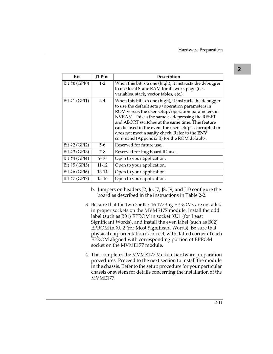
Bit | J1 Pins | Description |
|
|
|
Bit #0 (GPI0) | When this bit is a one (high), it instructs the debugger | |
|
| to use local Static RAM for its work page (i.e., |
|
| variables, stack, vector tables, etc.). |
|
|
|
Bit #1 (GPI1) | When this bit is a one (high), it instructs the debugger | |
|
| to use the default setup/operation parameters in |
|
| ROM versus the user setup/operation parameters in |
|
| NVRAM. This is the same as depressing the RESET |
|
| and ABORT switches at the same time. This feature |
|
| can be used in the event the user setup is corrupted or |
|
| does not meet a sanity check. Refer to the ENV |
|
| command (Appendix B) for the ROM defaults. |
|
|
|
Bit #2 (GPI2) | Reserved for future use. | |
|
|
|
Bit #3 (GPI3) | Reserved for bug board ID use. | |
|
|
|
Bit #4 (GPI4) | Open to your application. | |
|
|
|
Bit #5 (GPI5) | Open to your application. | |
|
|
|
Bit #6 (GPI6) | Open to your application. | |
|
|
|
Bit #7 (GPI7) | Open to your application. | |
|
|
|
b.Jumpers on headers J2, J6, J7, J8, J9, and J10 configure the board as described in the instructions in Table
3.Be sure that the two 256K x 16 177Bug EPROMs are installed in proper sockets on the MVME177 module. Install the odd label (such as B01) EPROM in socket XU1 (for Least Significant Words), and install the even label (such as B02) EPROM in XU2 (for Most Significant Words). Be sure that physical chip orientation is correct, with flatted corner of each EPROM aligned with corresponding portion of EPROM socket on the MVME177 module.
4.This completes the MVME177 Module hardware preparation procedures. Proceed to the next section to install the module in the chassis. Refer to the setup procedure for your particular chassis or system for details concerning the installation of the MVME177.
2 |