2 |
Hardware Preparation and Installation
Setup Instructions
Even though the MVME177Bug EPROMs are installed on the MVME177 module in the factory, follow this setup procedure for 177Bug to operate properly with the MVME177.
Inserting or removing modules while power is applied
! could damage module components.
Caution
1. Turn all equipment power OFF.
2. Refer to Table
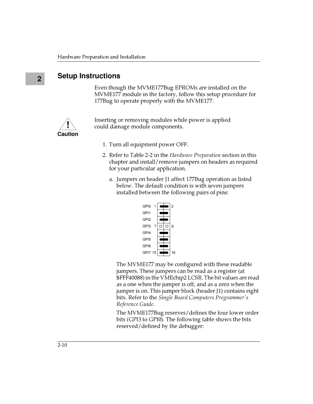
a. Jumpers on header J1 affect 177Bug operation as listed below. The default condition is with seven jumpers installed between the following pairs of pins:
GPI0 1 ![]() 2
2
GPI1
GPI2
GPI3 7 |
|
|
| 8 |
|
|
GPI4
GPI5
GPI6
GPI7 15 ![]()
![]() 16
16
The MVME177 may be configured with these readable jumpers. These jumpers can be read as a register (at $FFF40088) in the VMEchip2 LCSR. The bit values are read as a one when the jumper is off, and as a zero when the jumper is on. This jumper block (header J1) contains eight bits. Refer to the Single Board Computers Programmer's Reference Guide.
The MVME177Bug reserves/defines the four lower order bits (GPI3 to GPI0). The following table shows the bits reserved/defined by the debugger: