CLOCK OSC.
55MHz/
20MHz
Freescale Semiconductor, Inc.
Functional Description
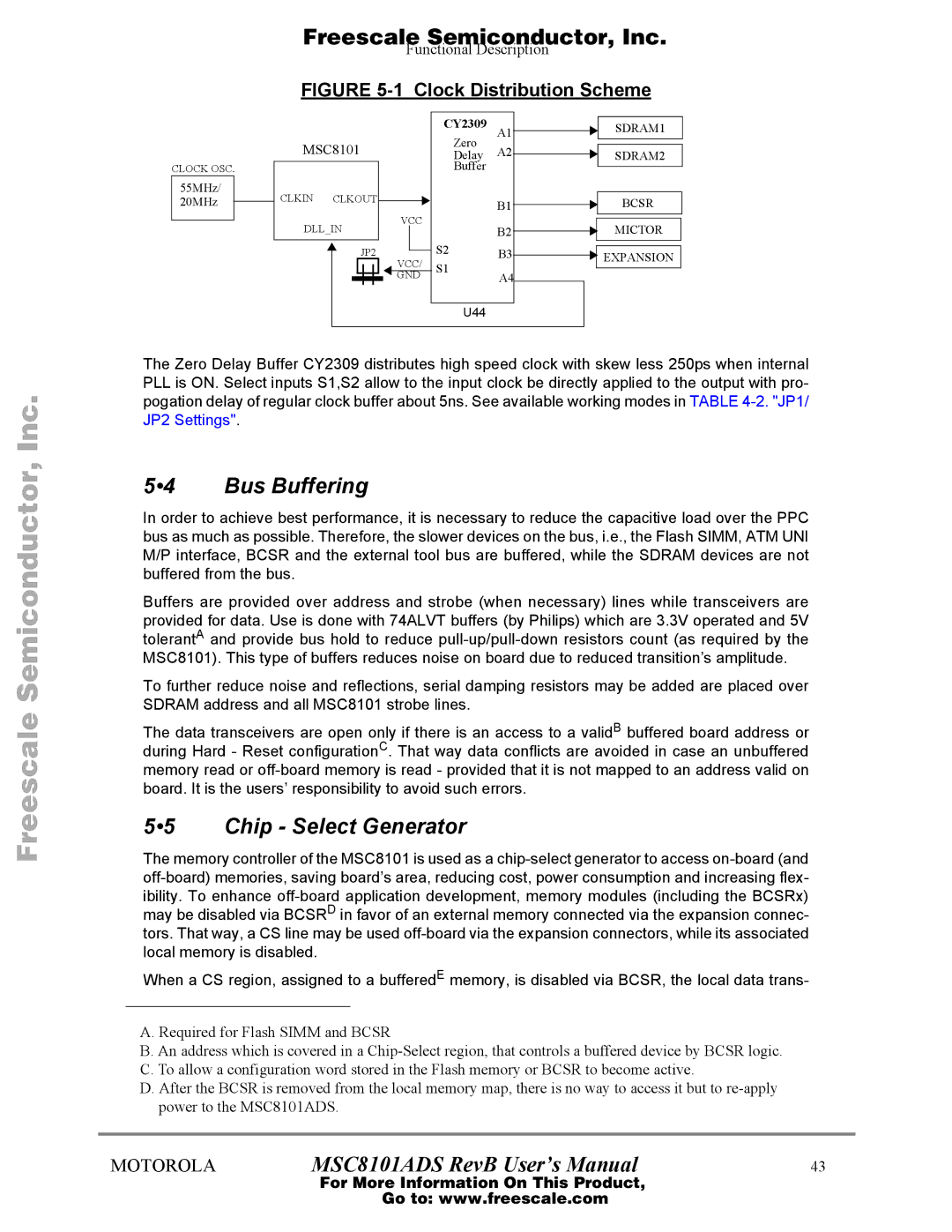
FIGURE 5-1 Clock Distribution Scheme
|
|
| CY2309 | A1 | SDRAM1 |
|
|
| Zero | ||
MSC8101 |
|
| |||
| A2 |
| |||
| Delay | SDRAM2 | |||
|
|
| Buffer |
|
|
CLKIN | CLKOUT |
|
| B1 | BCSR |
|
| VCC |
| ||
DLL_IN |
| B2 | MICTOR | ||
|
| ||||
| JP2 | VCC/ | S2 | B3 | EXPANSION |
|
| S1 | A4 |
| |
|
| GND |
|
| |
|
|
| U44 |
|
|
Freescale Semiconductor, Inc.
The Zero Delay Buffer CY2309 distributes high speed clock with skew less 250ps when internal PLL is ON. Select inputs S1,S2 allow to the input clock be directly applied to the output with pro- pogation delay of regular clock buffer about 5ns. See available working modes in TABLE
5•4 Bus Buffering
In order to achieve best performance, it is necessary to reduce the capacitive load over the PPC bus as much as possible. Therefore, the slower devices on the bus, i.e., the Flash SIMM, ATM UNI M/P interface, BCSR and the external tool bus are buffered, while the SDRAM devices are not buffered from the bus.
Buffers are provided over address and strobe (when necessary) lines while transceivers are provided for data. Use is done with 74ALVT buffers (by Philips) which are 3.3V operated and 5V tolerantA and provide bus hold to reduce
To further reduce noise and reflections, serial damping resistors may be added are placed over SDRAM address and all MSC8101 strobe lines.
The data transceivers are open only if there is an access to a validB buffered board address or during Hard - Reset configurationC. That way data conflicts are avoided in case an unbuffered memory read or
5•5 Chip - Select Generator
The memory controller of the MSC8101 is used as a
When a CS region, assigned to a bufferedE memory, is disabled via BCSR, the local data trans-
A. Required for Flash SIMM and BCSR
B. An address which is covered in a
D. After the BCSR is removed from the local memory map, there is no way to access it but to
MOTOROLA | MSC8101ADS RevB User’s Manual | 43 |
For More Information On This Product,
Go to: www.freescale.com
