MSC8101 ADS
MSC8101ADS RevB User’s Manual
Contents
ATM on LD14
BOM
Freescale Semiconductor, Inc
List of Figures
Viii
List of Tables
Freescale Semiconductor, Inc
Related Documentation
Introduction
Abbreviations’ List
Characteristics Specifications
Specification
MSC8101ADS Specifications
ADS Features
Freescale Semiconductor, Inc
Semiconductor, Inc
Hardware Preparation
MSC8101ADS Top Side Part Location diagram
Setting HReset Configuration Source
Setting The Core Supply Voltage Level
Setting MODCK13 For Initial PLLs’ Multiplication Factor SW9
OnCE Connection Scheme
Host I/F Operation
Stand Alone Operation
Host System Debug Scheme B
34 +5V Power Supply Connection
JTAG/OnCE Connector P6
Host I/F Connector P4
P6 JTAG/OnCE Port Connector
P4 Host I/F Connector
Terminal to MSC8101ADS RS-232 Connection
Flash Memory Simm Installation
38 10/100-Base-T Ethernet Port Connection
Flash Memory Simm Insertion
Host I/F Setting SW1
Emulator Enable EE SW2
Data Bus Width Setting SW5 & SW6
Abort Switch SW3
Soft Reset Sreset Switch SW4
Configuration Switch SW9
Hard Reset Hreset Switch SW7
Power-On Reset Switch Preset SW8
Available Clock Mode Setting
Boot Mode Select SW10
Modck
CPM
Software Options Switch SW11
431 JP1 DLL Disable
Jumpers
432 JP2 Clock Buffer Set
433 JP3 50 Ohm Enable
436 JP6,JP7 MIC Enable
437 JP9 5V power supply for Codec
434 JP4 VPP Source Selector
LEDs
Ethernet Link Indicator LD4
Fast Ethernet Clsn Indicator LD5
ATM RX Indicator LD6
ATM TX Indicator LD7
MSC8101’s Registers’ Programming
Memory Controller Registers Programming
SIU Registers’ Programming
System Initialization
Memory Controller Initialization for 10050a MHz
Memory Controller Initialization for 10050a MHz
Mbmr
Reset & Reset Configuration
Power- On Reset
Power On Reset Configuration
Manual Hard Reset
Summary Reset Configuration Schemes
Hard Reset Configuration Word
Manual Soft Reset
IRQ2
Local Interrupter
Clock Generator
Bus Buffering
Chip Select Generator
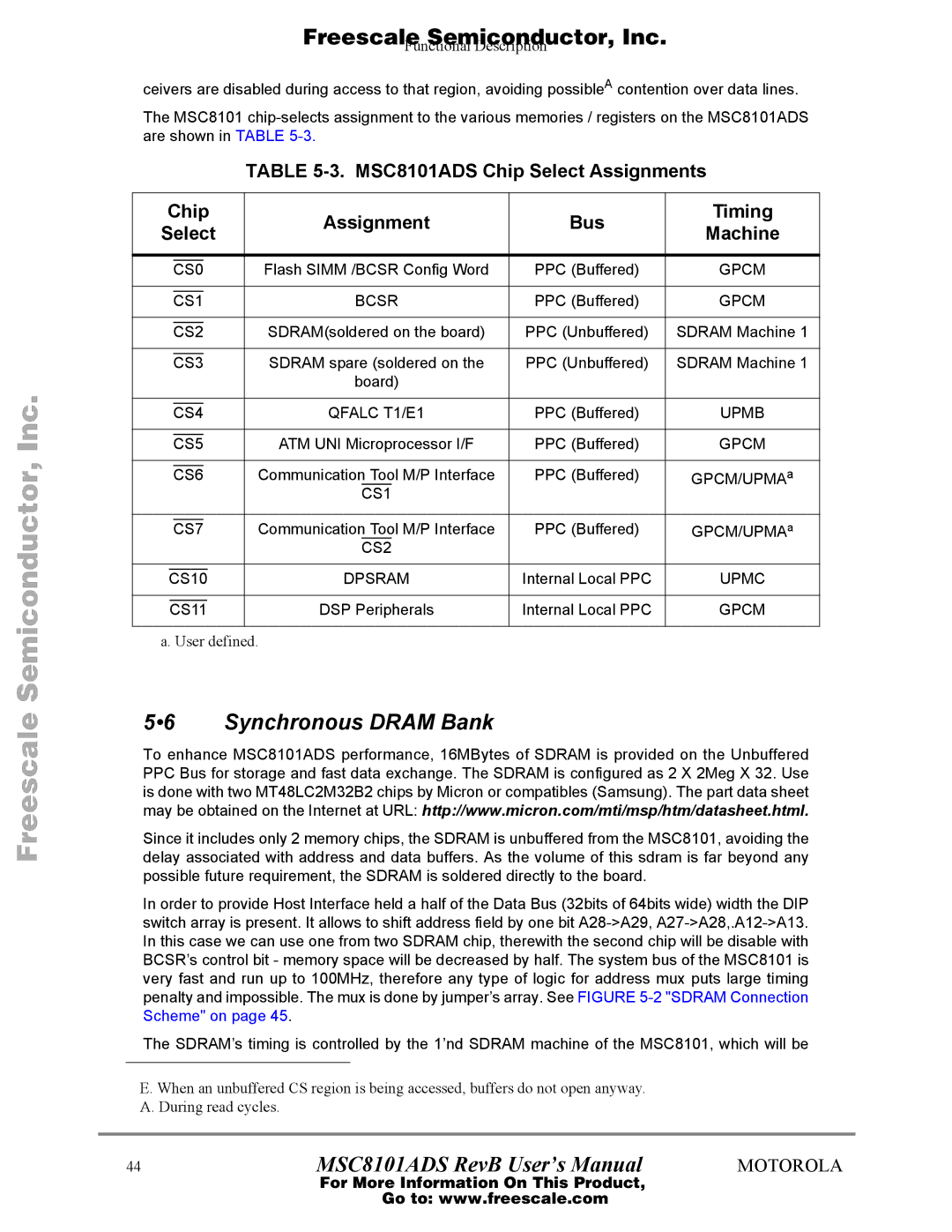
Synchronous Dram Bank
MSC8101ADS Chip Select Assignments Bus Timing Machine
Sdram
MHz Sdram Mode Register Programming
Sdram Programming
Sdram Refresh
Cycle Type \ Flash Delay nsec
Flash Memory Simm
Flash Simm Connection Scheme
Flash Programming Voltage
Communication Ports
Ports Function Enable
MSC8101 I/O Ports/Name
581 ATM Port
582 100/10 Base T Port
5831 CS4221 Programming
CS4221 Programming
Audio Codec
585 RS232 Ports
CS4221 Programming
584 T1/E1 Ports
Host I/F
Board Control & Status Register Bcsr
Host I/F Interconnect signals
DMA off-board tool
BCSR0 Description
BCSR0 Board Control / Status Register
BIT Mnemonic
PON ATT DEF Hostcsp
BCSR1 Board Control / Status Register
BCSR0 Description
10. BCSR1 Description
10. BCSR1 Description
PON ATT DEF Atmrst
Fethien
Fethrst
BCSR2 Board Control / Status Register
11. Peripheral’s Availability Decoding
12. BCSR2 Description
12. BCSR2 Description
13. Flash Presence Detect 75 Encoding
14. Flash Presence Detect 41 Encoding
BCSR3 Board Status Register
15. BCSR3 Description
16. EXTOOLI03 Assignment
17. External Tool Revision Encoding
18. ADS Revision Encoding
Engineering
PPC Bus Memory Map
MSC8101ADS Memory Map
MSC8101ADS Memory Map
FE000000 Ffffffff
FF000000 Ffffffff
FF800000 Ffffffff
Power rails
ADS Power Scheme
Off-Board Application Maximum Current Consumption
711 5V Bus
712 3V Bus
713 5V Bus
Appendix a MSC8101 Bill of Material
A1 BOM
Table A-1. MSC8101ADS Bill Of Material
Freescale
Inc
Inc
Dale
Freescale
Semiconductor
Freescale Semiconductor, Inc
Appendix B Support Information
Interconnect Signals
B11
Table B1-2. P1 System Expansion Interconnect Signals
GND
TSTAT0
TSTAT1
TSTAT2 TSTAT3 TSTAT4 TSTAT5
Clkx
Damage to the PM5350 ATM UNI
EXPD0
EXPD1
EXPD2
EXPD3
EXPCTL0
SCC1RXD PD30
Table B1-3. P2 CPM Expansion Interconnect Signals
B12 MSC8101ADS’s P2 CPM Expansion Connector
SPICLKPD18
SPIMOSIPD17
Hwrds
PD7
Atmtsoc PA29
Atmrsoc PA27
Atmrfclk
Atmrca PA26
ATMRXD7 PA17
ATMRXD6 PA16
ATMRXD5 PA15
ATMRXD4 PA14
Fethtxen PB29
Fethrxer PB28
Fethcol PB27
Fethcrs PB26
HD0
HD1
HD2
HD3
Atmfclk PC26
Fethmdc PC13
Fethmdio PC12
PC7
PC6
SMCTX1PC5
B13
Table B1-4. P3 ISP Connector Interconnect Signals
B14 P4 Host Interface Connector
HD1 HD2 HD3 HD4 HD5 HD6 HD7 HD8 HD9
HA1 HA2 HA3 HCS1
Hack
Hreq
Table B1-6. P6 JTAG/ONCE Connector Interconnect Signals
B15 P5, P7, P8, P9, P10, P13, P14 Logic Analyzer Connectors
B16
HDS
Table B1-7. P12 Ethernet Port Interconnect Signals
B17 P12 Ethernet Port Connector
B18 P15,P16 SMB Connectors
B19 P17,P18 Double RJ45 T1/E1 Line Connectors
B110 P19,P21,P24 Stereo Phone Jack Connectors
B111 P20,P22,P23,P25 RCA Jack Connectors
Table B1-10. P27A Interconnect Signals
Table B1-11. P27B Interconnect Signals
B112 P26 5V Power Supply Connectors
B113 P27A,B RS232 Ports’ Connectors
Freescale Semiconductor, Inc
Appendix C Program Information
Freescale Semiconductor, Inc
Logic Equations
C11 First Include File
C12 Second Include file
C13 Main File
Constant SHIFTLENGTH= Length of HRD/HRW Delay Shifter SIZE0
Constant EE45HOLDVALUE
Constant SIZE1
Constant
Constant TCPCDEFAULT0 Constant TCPCDEFAULT1
HDIMDEN~ Host SW Enable RSTCNF~ Output
SRESET~
HRESET~ Bidir
SBOOTENOUT~
SPARE1 Output
HDIEN~
HRRQEN~
WDTIMER1
WDTIMER2
WDTIMER3
WDTIMER4
Eepromenable
Resets Cleartowdctrl
BCSR1 SBOOTEN~
Scndcfgbyteread Thirdcfgbyteread Fourthcfgbyteread
BCSR3
IRQ0
BCSR1PONDEF0..SIZE1
BCSR3PONDEF0..SIZE3
BCSR0 BCSR0PONCONST0..5
Begin Defaults
END Defaults
END if END Generate
EEDPONDEFAULT,RSV37PONDEFAULT
Else
EE Pins
Regularpoweronreset = RPORI~ == Regularponresetactive
PSDVAL~ = Opndrnvcc
END if
If Hdds then
If !HDSP then Hdiwr =
Else Hdiwr =
END if Else
Elsif MPCWRITEBCSR1 then
Elsif MPCWRITEBCSR4 then
Elsif MPCWRITEBCSR5 then
Elsif MPCWRITEBCSR6 then
Elsif MPCREADBCSR3 then
SIGNALLAMP1~ Elsif MPCREADBCSR1 then
If MPCREADBCSR0 then
HRESET~ =
SRESET~ =
Elsif Firstcfgbyteread then
Elsif Scndcfgbyteread then
Then SIGLAMP0OUT~ = GND Else
Then SIGLAMP1OUT~
Else SIGLAMP1OUT~
END if If !T1234EN~ & FETHIEN~ then
116
MODCK1-3 Driven
END if Drive Poreset Impulse Reconfig Using BCSR4
Watchdog for Auto Reconfiguration
118