Freescale Semiconductor, Inc.
Freescale Semiconductor, Inc.
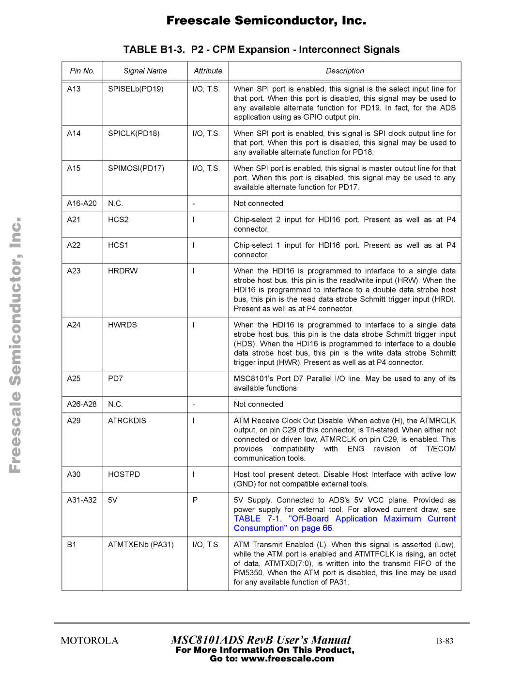
TABLE B1-3. P2 - CPM Expansion - Interconnect Signals
Pin No. | Signal Name | Attribute | Description |
|
|
|
|
|
|
|
|
A13 | SPISELb(PD19) | I/O, T.S. | When SPI port is enabled, this signal is the select input line for |
|
|
| that port. When this port is disabled, this signal may be used to |
|
|
| any available alternate function for PD19. In fact, for the ADS |
|
|
| application using as GPIO output pin. |
|
|
|
|
A14 | SPICLK(PD18) | I/O, T.S. | When SPI port is enabled, this signal is SPI clock output line for |
|
|
| that port. When this port is disabled, this signal may be used to |
|
|
| any available alternate function for PD18. |
|
|
|
|
A15 | SPIMOSI(PD17) | I/O, T.S. | When SPI port is enabled, this signal is master output line for that |
|
|
| port. When this port is disabled, this signal may be used to any |
|
|
| available alternate function for PD17. |
|
|
|
|
N.C. | - | Not connected | |
|
|
|
|
A21 | HCS2 | I | |
|
|
| connector. |
|
|
|
|
A22 | HCS1 | I | |
|
|
| connector. |
|
|
|
|
A23 | HRDRW | I | When the HDI16 is programmed to interface to a single data |
|
|
| strobe host bus, this pin is the read/write input (HRW). When the |
|
|
| HDI16 is programmed to interface to a double data strobe host |
|
|
| bus, this pin is the read data strobe Schmitt trigger input (HRD). |
|
|
| Present as well as at P4 connector. |
|
|
|
|
A24 | HWRDS | I | When the HDI16 is programmed to interface to a single data |
|
|
| strobe host bus, this pin is the data strobe Schmitt trigger input |
|
|
| (HDS). When the HDI16 is programmed to interface to a double |
|
|
| data strobe host bus, this pin is the write data strobe Schmitt |
|
|
| trigger input (HWR). Present as well as at P4 connector. |
|
|
|
|
A25 | PD7 |
| MSC8101’s Port D7 Parallel I/O line. May be used to any of its |
|
|
| available functions |
|
|
|
|
N.C. | - | Not connected | |
|
|
|
|
A29 | ATRCKDIS | I | ATM Receive Clock Out Disable. When active (H), the ATMRCLK |
|
|
| output, on pin C29 of this connector, is |
|
|
| connected or driven low, ATMRCLK on pin C29, is enabled. This |
|
|
| provides compatibility with ENG revision of T/ECOM |
|
|
| communication tools. |
|
|
|
|
A30 | HOSTPD | I | Host tool present detect. Disable Host Interface with active low |
|
|
| (GND) for not compatible external tools. |
|
|
|
|
5V | P | 5V Supply. Connected to ADS’s 5V VCC plane. Provided as | |
|
|
| power supply for external tool. For allowed current draw, see |
|
|
| TABLE |
|
|
| Consumption" on page 66. |
|
|
|
|
B1 | ATMTXENb (PA31) | I/O, T.S. | ATM Transmit Enabled (L). When this signal is asserted (Low), |
|
|
| while the ATM port is enabled and ATMTFCLK is rising, an octet |
|
|
| of data, ATMTXD(7:0), is written into the transmit FIFO of the |
|
|
| PM5350. When the ATM port is disabled, this line may be used |
|
|
| for any available function of PA31. |
|
|
|
|
MOTOROLA | MSC8101ADS RevB User’s Manual |
For More Information On This Product,
Go to: www.freescale.com
