Freescale Semiconductor, Inc.
Freescale Semiconductor, Inc.
Functional Description
b. Two clocks latency setting is programmed for 50MHz Bus Clock
c. 8 beat burst is programmed for 32bit Data Bus width (Host Interface is active)
5•6•2 SDRAM Refresh
The SDRAM is refreshed using its
5•7 Flash Memory SIMM
The MSC8101 is provided with 8Mbyte of 90 nsec flash memory SIMM, the SM73228XG1JHBGO by Smart Modular Technology which is composed of four
To minimize use of MSC8101s’
The access time of the Flash memory provided with the MSC8101ADS is 95 nsec, however, devices with different delay are supported as well. By reading the delay section of the Flash SIMM
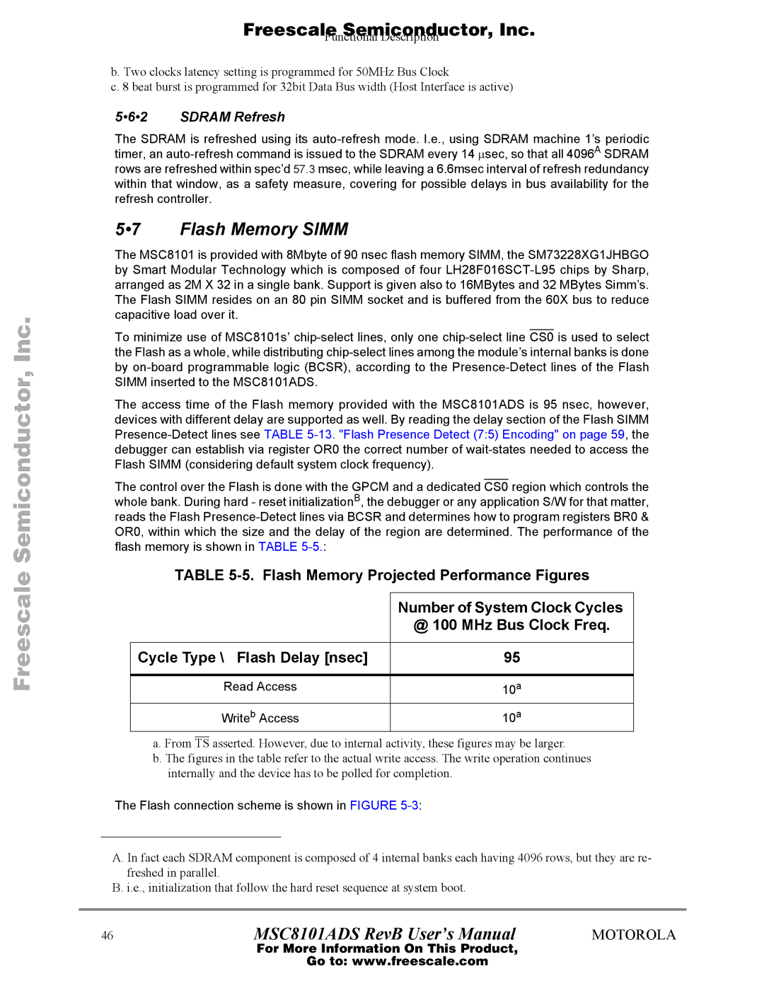
The control over the Flash is done with the GPCM and a dedicated CS0 region which controls the whole bank. During hard - reset initializationB, the debugger or any application S/W for that matter, reads the Flash
TABLE
| Number of System Clock Cycles |
| @ 100 MHz Bus Clock Freq. |
|
|
Cycle Type \ Flash Delay [nsec] | 95 |
|
|
Read Access | 10a |
Writeb Access | 10a |
a. From TS asserted. However, due to internal activity, these figures may be larger.
b. The figures in the table refer to the actual write access. The write operation continues internally and the device has to be polled for completion.
The Flash connection scheme is shown in FIGURE 5-3:
A. In fact each SDRAM component is composed of 4 internal banks each having 4096 rows, but they are re- freshed in parallel.
B. i.e., initialization that follow the hard reset sequence at system boot.
46MSC8101ADS RevB User’s Manual MOTOROLA
For More Information On This Product,
Go to: www.freescale.com
