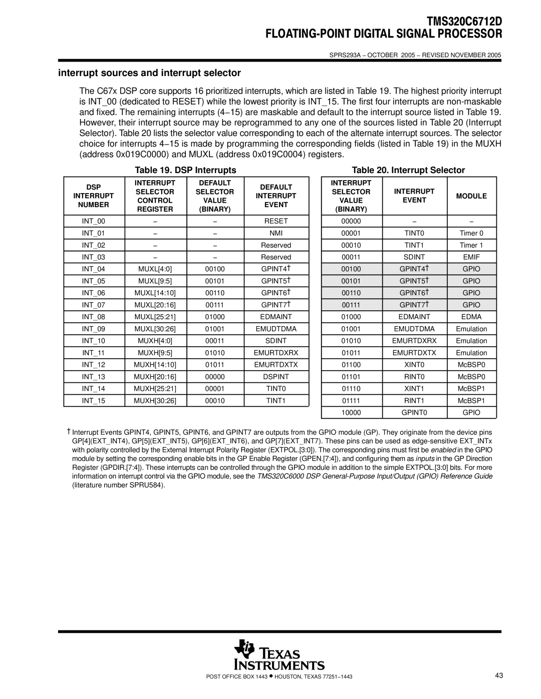
TMS320C6712D specifications
The Texas Instruments TMS320C6712D is a high-performance, fixed-point digital signal processor (DSP) that belongs to the TMS320C6000 family, well known for its advanced processing capabilities tailored for demanding signal processing applications. Launched in the early 2000s, the C6712D combines high computational power with a rich set of features, making it suitable for a variety of applications such as telecommunications, audio processing, and industrial control systems.One of the standout characteristics of the TMS320C6712D is its architecture, which is based on a highly efficient VLIW (Very Long Instruction Word) design. This architecture allows the processor to execute multiple instructions in a single clock cycle, significantly increasing performance. The device operates at clock speeds of up to 150 MHz, providing substantial computational throughput that can handle complex algorithms and real-time processing tasks.
Another key feature of the TMS320C6712D is its 32-bit fixed-point processing capabilities, which allows it to perform difficult mathematical computations efficiently. With an instruction set optimized for DSP applications, the processor includes specialized instructions for multiplying and accumulating operations, as well as support for advanced filtering and generation of audio signals.
The C6712D offers an extensive memory architecture, supporting up to 128 MB of external memory via a 32-bit data bus. It features on-chip SRAM, which provides fast access to data and program storage, enhancing the system's overall performance. Additionally, the device includes a powerful set of peripherals, such as dual asynchronous serial ports (UART), I2C interfaces, and DSP-specific interfaces that facilitate connectivity with other components and systems.
Power consumption is another vital aspect of the TMS320C6712D. It incorporates technologies allowing for low-power operation, which is essential for portable and battery-operated devices. The capability to operate in various power modes helps optimize performance while minimizing energy usage.
In conclusion, the Texas Instruments TMS320C6712D is a versatile and powerful DSP that excels in high-performance applications. Its VLIW architecture, fixed-point processing capabilities, extensive memory options, and low power consumption make it an ideal choice for engineers looking to implement complex signal processing tasks efficiently. Whether used in telecommunications, audio processing, or industrial applications, the C6712D remains a reliable and capable solution in the digital signal processing landscape.

