4-2. Sub Screen Process Section
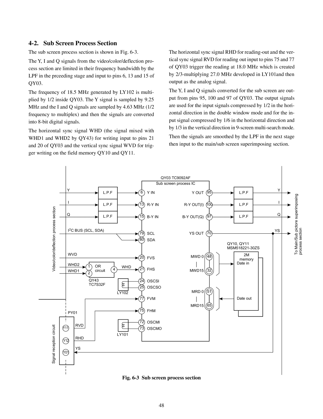
The sub screen process section is shown in Fig.
The Y, I and Q signals from the video/color/deflection pro- cess section are limited in their frequency bandwidth by the LPF in the prceeding stage and input to pins 6, 13 and 15 of QY03.
The frequency of 18.5 MHz generated by LY102 is multi- plied by 1/2 inside QY03. The Y signal is sampled by 9.25 MHz and the I and Q signals are sampled by 4.63 MHz (1/2 frequency to multiplex) and then the signals are converted into
The horizontal sync signal WHD (the signal mixed with WHD1 and WHD2 by QY43) for writing input to pins 21 and 20 of QY03 and the vertical sync signal WVD for trig- ger writing on the field memory QY10 and QY11.
The horizontal sync signal RHD for
The Y, I and Q signals converted for the sub screen are out- put from pins 95, 100 and 97 of QY03. The output signals are used for the input signals compressed by 1/2 in the hori- zontal direction in the double window mode and for the in- put signal compressed by 1/6 in the horizontal direction and by 1/3 in the vertical direction in
Then the signals are smoothed by the LPF in the next stage then input to the main/sub screen superimposing section.
Video/color/deflection process section
Signal reception circuit
|
|
|
| QY03 TC9092AF |
|
|
|
|
|
| Sub screen process IC |
|
|
| |
Y | L.P.F | 6 | Y IN | Y OUT | 95 | L.P.F | Y |
|
| ||||||
I | L.P.F | 13 | 100 | L.P.F | I | ||
|
| ||||||
Q | L.P.F | 15 | 97 | L.P.F | Q | ||
|
| ||||||
I2C BUS (SCL, SDA) |
|
| 79 | SCL | YS OUT | 70 | YS | |||
|
|
|
|
|
|
| ||||
|
|
|
|
|
| 80 | SDA |
|
| QY10, QY11 |
|
|
|
|
|
|
|
|
|
| |
|
|
|
|
|
|
|
|
|
| |
WVD |
|
|
|
| 20 | FVS | MWD 0 | 48 | 2M | |
|
|
|
|
|
| memory | ||||
|
|
|
|
|
|
|
|
|
| |
WHD2 | 1 | OR |
| WHD |
|
|
|
| Date in | |
|
|
|
|
|
| |||||
|
| 4 | 21 | FHS |
| 32 |
| |||
WHD1 | 2 | circuit |
| MWD15 |
| |||||
|
|
|
|
| ||||||
|
|
|
|
|
|
|
|
|
| |
|
| QY43 |
|
| 24 | OSCSI |
|
|
| |
|
| TC7S32F |
|
| 25 | OSCSO |
|
|
| |
|
|
|
|
|
|
|
|
| ||
|
|
|
|
| LY102 |
|
| MRD 0 | 51 |
|
|
|
|
|
|
|
|
|
|
| |
|
|
|
|
|
| 77 | FVM |
|
| Date out |
|
|
|
|
|
|
|
| MRD15 | 65 |
|
PY01 |
|
|
|
| 75 | FHM |
|
|
| |
|
|
|
|
|
|
|
|
| ||
| RVD |
|
|
|
| 72 | OSCMI |
|
|
|
Y11 |
|
|
|
| 73 | OSCMO |
|
|
| |
|
|
|
|
|
|
|
| |||
| RHD |
|
|
| LY101 |
|
|
|
|
|
Y12 |
|
|
|
|
|
|
|
|
| |
|
|
|
|
|
|
|
|
|
| |
Y01 | YS |
|
|
|
|
|
|
|
|
|
|
|
|
|
|
|
|
|
|
| |
To Main/Sub pictore superimposing process section
Fig. 6-3 Sub screen process section
48