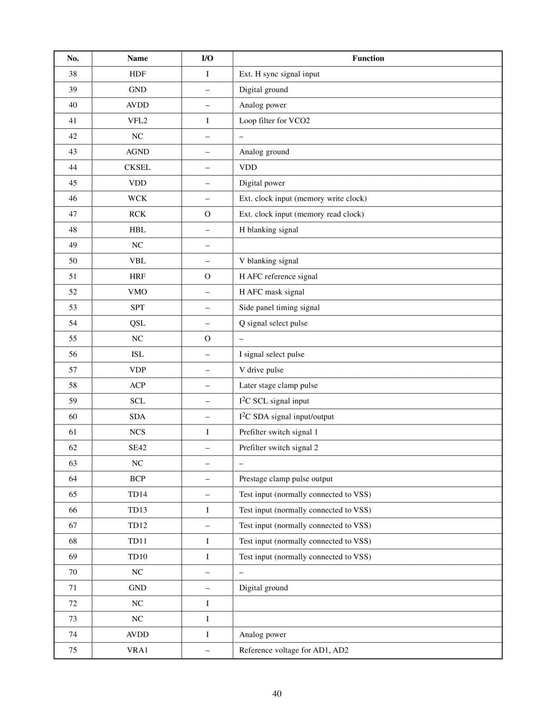
No.
38
39
40
41
42
43
44
45
46
47
48
49
50
51
52
53
54
55
56
57
58
59
60
61
62
63
64
65
66
67
68
69
70
71
72
73
74
75
Name | I/O | Function |
|
|
|
HDF | I | Ext. H sync signal input |
|
|
|
GND | – | Digital ground |
|
|
|
AVDD | – | Analog power |
|
|
|
VFL2 | I | Loop filter for VCO2 |
|
|
|
NC | – | – |
|
|
|
AGND | – | Analog ground |
|
|
|
CKSEL | – | VDD |
|
|
|
VDD | – | Digital power |
|
|
|
WCK | – | Ext. clock input (memory write clock) |
|
|
|
RCK | O | Ext. clock input (memory read clock) |
|
|
|
HBL | – | H blanking signal |
|
|
|
NC | – |
|
|
|
|
VBL | – | V blanking signal |
|
|
|
HRF | O | H AFC reference signal |
|
|
|
VMO | – | H AFC mask signal |
|
|
|
SPT | – | Side panel timing signal |
|
|
|
QSL | – | Q signal select pulse |
|
|
|
NC | O | – |
|
|
|
ISL | – | I signal select pulse |
|
|
|
VDP | – | V drive pulse |
|
|
|
ACP | – | Later stage clamp pulse |
|
|
|
SCL | – | I2C SCL signal input |
SDA | – | I2C SDA signal input/output |
NCS | I | Prefilter switch signal 1 |
|
|
|
SE42 | – | Prefilter switch signal 2 |
|
|
|
NC | – | – |
|
|
|
BCP | – | Prestage clamp pulse output |
|
|
|
TD14 | – | Test input (normally connected to VSS) |
|
|
|
TD13 | I | Test input (normally connected to VSS) |
|
|
|
TD12 | – | Test input (normally connected to VSS) |
|
|
|
TD11 | I | Test input (normally connected to VSS) |
|
|
|
TD10 | I | Test input (normally connected to VSS) |
|
|
|
NC | – | – |
|
|
|
GND | – | Digital ground |
|
|
|
NC | I |
|
|
|
|
NC | I |
|
|
|
|
AVDD | I | Analog power |
|
|
|
VRA1 | – | Reference voltage for AD1, AD2 |
|
|
|
|
|
|
40