3. ACTUAL CIRCUIT
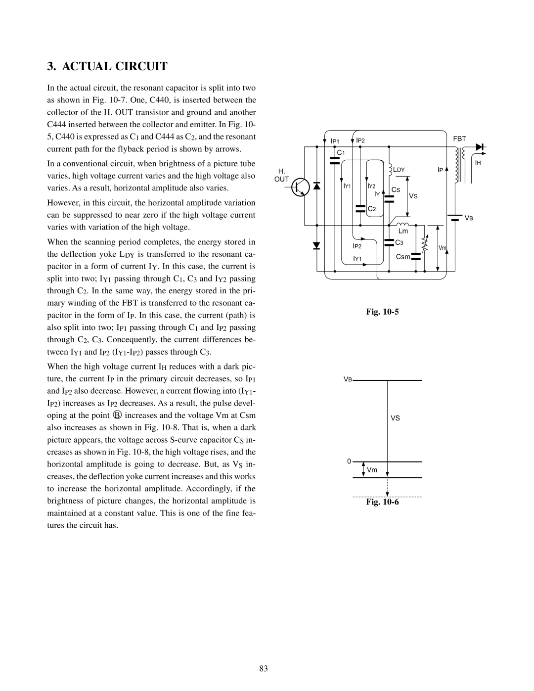
In the actual circuit, the resonant capacitor is split into two as shown in Fig.
In a conventional circuit, when brightness of a picture tube varies, high voltage current varies and the high voltage also varies. As a result, horizontal amplitude also varies.
However, in this circuit, the horizontal amplitude variation can be suppressed to near zero if the high voltage current varies with variation of the high voltage.
When the scanning period completes, the energy stored in the deflection yoke LDY is transferred to the resonant ca- pacitor in a form of current IY. In this case, the current is split into two; IY1 passing through C1, C3 and IY2 passing through C2. In the same way, the energy stored in the pri- mary winding of the FBT is transferred to the resonant ca- pacitor in the form of IP. In this case, the current (path) is also split into two; IP1 passing through C1 and IP2 passing through C2, C3. Concequently, the current differences be- tween IY1 and IP2
When the high voltage current IH reduces with a dark pic- ture, the current IP in the primary circuit decreases, so IP1 and IP2 also decrease. However, a current flowing into (IY1- IP2) increases as IP2 decreases. As a result, the pulse devel- oping at the point B increases and the voltage Vm at Csm also increases as shown in Fig.
H.
OUT
IP1 | IP2 |
|
| FBT |
C1 |
|
|
|
|
|
|
| LDY | IH |
|
|
| IP | |
IY1 |
| IY2 | CS |
|
|
| IY |
| |
|
| VS |
| |
|
|
|
| |
|
| C2 |
|
|
|
|
|
| VB |
|
|
| Lm |
|
| IP2 |
| C3 | Vm |
|
|
| ||
|
|
|
| |
| IY1 |
| Csm |
|
|
|
|
|
Fig.
VB
VS
0
Vm
Fig.
83