2-3. V Output
2-3-1. Circuit Operation
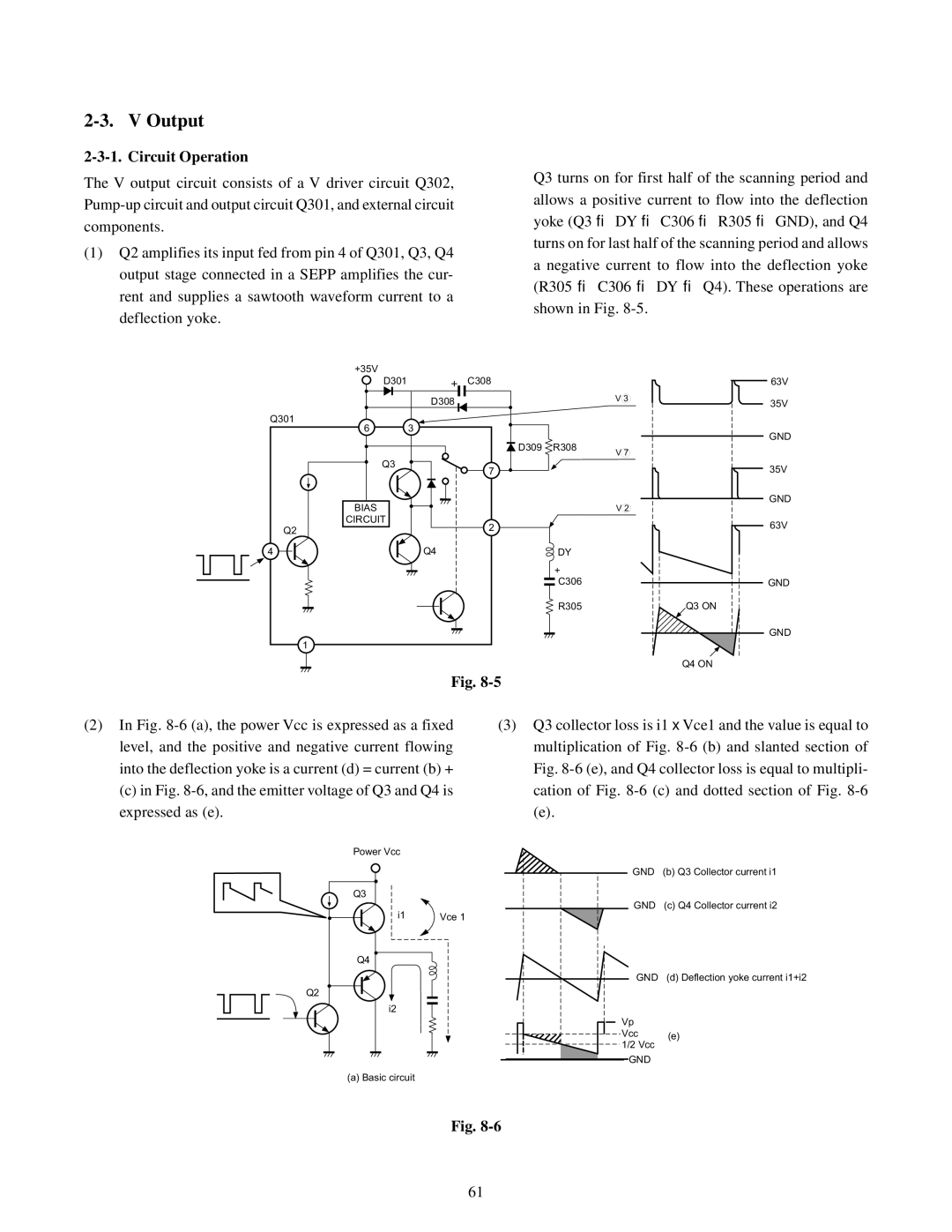
The V output circuit consists of a V driver circuit Q302,
(1)Q2 amplifies its input fed from pin 4 of Q301, Q3, Q4 output stage connected in a SEPP amplifies the cur- rent and supplies a sawtooth waveform current to a deflection yoke.
Q3 turns on for first half of the scanning period and allows a positive current to flow into the deflection yoke (Q3 ® DY ® C306 ® R305 ® GND), and Q4 turns on for last half of the scanning period and allows a negative current to flow into the deflection yoke (R305 ® C306 ® DY ® Q4). These operations are shown in Fig.
+35V |
|
|
|
|
D301 | C308 |
|
| 63V |
| D308 |
| V 3 | 35V |
|
|
| ||
Q301 |
|
|
|
|
6 | 3 |
|
| GND |
|
|
|
| |
| D309 | R308 | V 7 |
|
|
|
|
| |
Q3 | 7 |
|
| 35V |
|
|
| ||
BIAS |
|
| V 2 | GND |
|
|
| ||
CIRCUIT | 2 |
|
| 63V |
Q2 |
|
| ||
|
|
|
| |
4 | Q4 | DY |
|
|
|
| + |
|
|
|
| C306 |
| GND |
|
| R305 |
| Q3 ON |
|
|
|
| GND |
1 |
|
|
|
|
|
|
|
| Q4 ON |
| Fig. |
|
|
|
(2)In Fig.
(c) in Fig.
Power Vcc
Q3
i1 | Vce 1 |
Q4
Q2
i2
(a) Basic circuit
(3)Q3 collector loss is i1 x Vce1 and the value is equal to multiplication of Fig.
(e).
GND (b) Q3 Collector current i1
GND (c) Q4 Collector current i2
GND (d) Deflection yoke current i1+i2
Vp
Vcc (e)
1/2 Vcc
![]() GND
GND
Fig.
61