3-1. Basic Operation and Current Path
3-1-1. Later Half Scanning Period
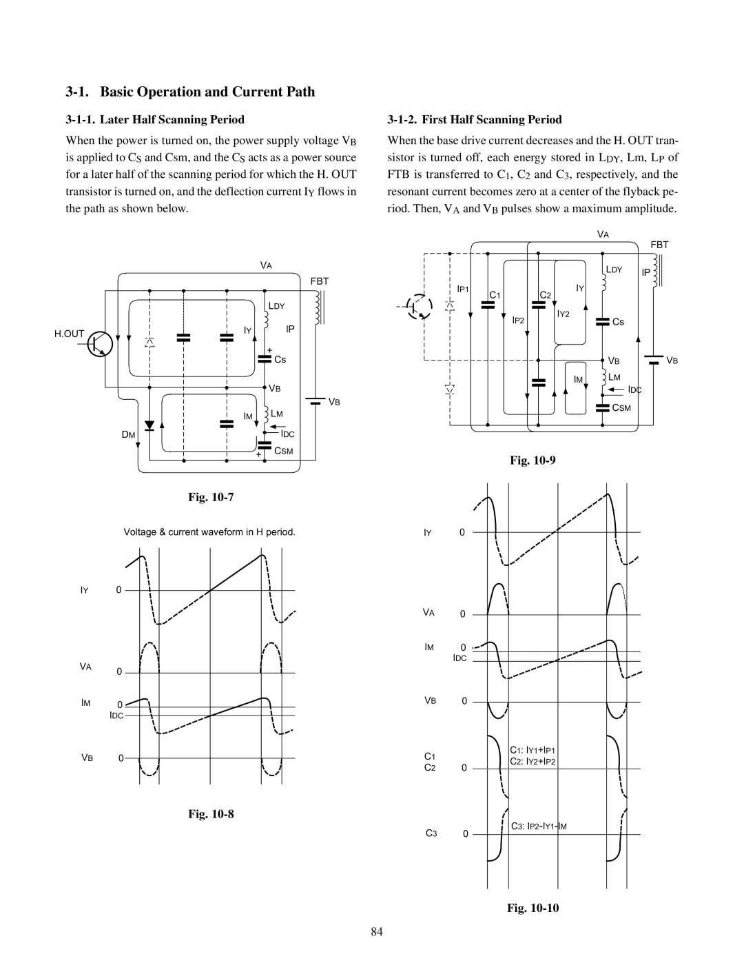
When the power is turned on, the power supply voltage VB is applied to CS and Csm, and the CS acts as a power source for a later half of the scanning period for which the H. OUT transistor is turned on, and the deflection current IY flows in the path as shown below.
|
| VA | |
|
|
| FBT |
|
|
| LDY |
H.OUT | IY |
| lP |
|
|
| |
|
|
| + |
|
|
| Cs |
|
|
| VB |
|
|
| VB |
| IM |
| LM |
|
|
| |
| DM |
| IDC |
|
| + | CSM |
3-1-2. First Half Scanning Period
When the base drive current decreases and the H. OUT tran- sistor is turned off, each energy stored in LDY, Lm, LP of FTB is transferred to C1, C2 and C3, respectively, and the resonant current becomes zero at a center of the flyback pe- riod. Then, VA and VB pulses show a maximum amplitude.
VA
FBT
LDY lP
IP1 | C1 | IY |
| ||
| C2 |
| |||
| IP2 | IY2 |
| ||
|
|
|
| Cs | |
VB |
|
|
| VB |
IM LM
IDC
![]()
![]() CSM
CSM
Fig.
Voltage & current waveform in H period.
IY 0
VA 0
IM 0 ![]()
IDC
VB 0
Fig.
IY 0
VA 0
IM 0
IDC
VB 0
C1
C2 0
C3 0
Fig.
C1: IY1+IP1
C2: IY2+IP2
![]() C3:
C3:
Fig.
84