SECTION IX: HORIZONTAL DEFLECTION CIRCUIT
1. OUTLINE
The H deflection circuit works to deflect a beam from left to right by flowing a sawtooth waveform of 15.625 kHz/15.735 kHz into the DY H deflection coil.
2. HORIZONTAL DRIVE CIRCUIT
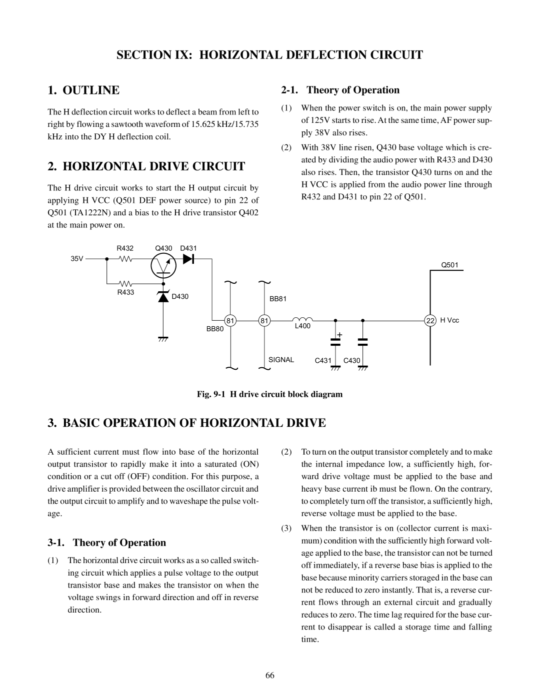
The H drive circuit works to start the H output circuit by applying H VCC (Q501 DEF power source) to pin 22 of Q501 (TA1222N) and a bias to the H drive transistor Q402 at the main power on.
2-1. Theory of Operation
(1)When the power switch is on, the main power supply of 125V starts to rise. At the same time, AF power sup- ply 38V also rises.
(2)With 38V line risen, Q430 base voltage which is cre- ated by dividing the audio power with R433 and D430 also rises. Then, the transistor Q430 turns on and the H VCC is applied from the audio power line through R432 and D431 to pin 22 of Q501.
R432 | Q430 | D431 |
|
|
35V |
|
|
|
|
R433 | D430 |
| BB81 | |
|
| |||
|
|
|
| |
|
| 81 | 81 | L400 |
|
| BB80 |
| |
|
|
|
| |
Q501
22 H Vcc
SIGNAL |
|
|
|
|
|
C431 C430 |
| ||||
|
|
|
|
|
|
|
|
|
|
|
|
Fig. 9-1 H drive circuit block diagram
3. BASIC OPERATION OF HORIZONTAL DRIVE
A sufficient current must flow into base of the horizontal output transistor to rapidly make it into a saturated (ON) condition or a cut off (OFF) condition. For this purpose, a drive amplifier is provided between the oscillator circuit and the output circuit to amplify and to waveshape the pulse volt- age.
3-1. Theory of Operation
(1)The horizontal drive circuit works as a so called switch- ing circuit which applies a pulse voltage to the output transistor base and makes the transistor on when the voltage swings in forward direction and off in reverse direction.
(2)To turn on the output transistor completely and to make the internal impedance low, a sufficiently high, for- ward drive voltage must be applied to the base and heavy base current ib must be flown. On the contrary, to completely turn off the transistor, a sufficiently high, reverse voltage must be applied to the base.
(3)When the transistor is on (collector current is maxi- mum) condition with the sufficiently high forward volt- age applied to the base, the transistor can not be turned off immediately, if a reverse base bias is applied to the base because minority carriers storaged in the base can not be reduced to zero instantly. That is, a reverse cur- rent flows through an external circuit and gradually reduces to zero. The time lag required for the base cur- rent to disappear is called a storage time and falling time.
66