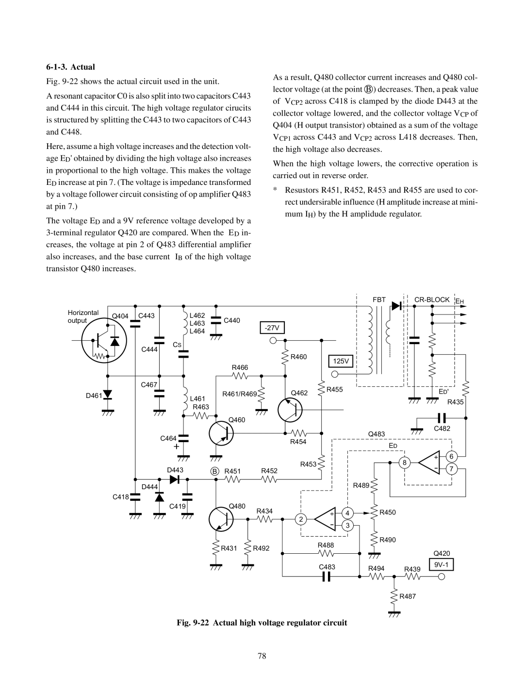
6-1-3. Actual
Fig. 9-22 shows the actual circuit used in the unit.
A resonant capacitor C0 is also split into two capacitors C443 and C444 in this circuit. The high voltage regulator cirucits is structured by splitting the C443 to two capacitors of C443 and C448.
Here, assume a high voltage increases and the detection volt- age ED' obtained by dividing the high voltage also increases in proportional to the high voltage. This makes the voltage ED increase at pin 7. (The voltage is impedance transformed by a voltage follower circuit consisting of op amplifier Q483 at pin 7.)
The voltage ED and a 9V reference voltage developed by a 3-terminal regulator Q420 are compared. When the ED in- creases, the voltage at pin 2 of Q483 differential amplifier also increases, and the base current IB of the high voltage transistor Q480 increases.
As a result, Q480 collector current increases and Q480 col- lector voltage (at the point B ) decreases. Then, a peak value of VCP2 across C418 is clamped by the diode D443 at the collector voltage lowered, and the collector voltage VCP of Q404 (H output transistor) obtained as a sum of the voltage VCP1 across C443 and VCP2 across L418 decreases. Then, the high voltage also decreases.
When the high voltage lowers, the corrective operation is carried out in reverse order.
*Resustors R451, R452, R453 and R455 are used to cor- rect undersirable influence (H amplitude increase at mini- mum IH) by the H amplidude regulator.
FBT |
|
| ||
|
|
|
|
|
Horizontal | Q404 | C443 |
| L462 |
|
|
|
|
|
|
|
output |
| C440 |
|
|
|
|
|
| |||
|
|
| L463 |
|
|
|
|
|
| ||
|
|
|
|
|
|
|
|
|
| ||
|
|
|
| L464 |
|
|
|
|
|
| |
|
|
|
|
|
|
|
|
|
|
| |
|
| C444 | CS |
|
|
|
|
|
|
|
|
|
|
|
|
|
|
|
|
|
|
| |
|
|
|
|
|
|
| R460 | 125V |
|
|
|
|
|
|
|
| R466 |
|
|
|
|
| |
|
|
|
|
|
|
|
|
|
|
| |
|
| C467 |
|
|
|
|
| R455 |
|
| ED’ |
D461 |
|
|
|
| R461/R469 | Q462 |
|
| |||
|
|
|
|
|
|
| |||||
|
|
| L461 |
|
|
| R435 | ||||
|
|
|
|
|
|
|
|
|
| ||
|
|
|
| R463 |
|
|
|
|
|
| |
|
|
|
|
|
|
|
|
|
|
| |
|
|
|
|
| Q460 |
|
|
|
|
|
|
|
|
|
|
|
|
|
|
| Q483 |
| C482 |
|
|
| C464 |
|
|
|
|
|
|
| |
|
|
|
|
|
| R454 |
|
|
|
| |
|
|
|
|
|
|
|
| ED |
|
| |
|
|
|
|
|
|
|
|
|
|
| |
|
|
|
|
|
|
|
|
|
| 8 | 6 |
|
|
| D443 |
| R451 | R452 | R453 |
|
| 7 | |
|
|
| B |
|
|
|
| ||||
|
| D444 |
|
|
|
|
|
| R489 |
|
|
| C418 |
|
|
|
|
|
|
|
|
|
|
|
|
| C419 |
| Q480 | R434 |
| 4 | R450 |
|
|
|
|
|
|
|
| 2 |
|
| |||
|
|
|
|
|
|
| 3 |
|
|
| |
|
|
|
|
|
|
|
|
|
|
| |
|
|
|
|
|
|
|
| R488 | R490 |
|
|
|
|
|
|
| R431 | R492 |
|
|
|
| |
|
|
|
|
|
|
|
|
| Q420 | ||
|
|
|
|
|
|
|
|
|
|
| |
|
|
|
|
|
|
|
| C483 | R494 | R439 | |
|
|
|
|
|
|
|
|
| |||
|
|
|
|
|
|
|
|
|
| R487 |
|
Fig. 9-22 Actual high voltage regulator circuit
78