4-3. H Blanking
4-3-1. Outline
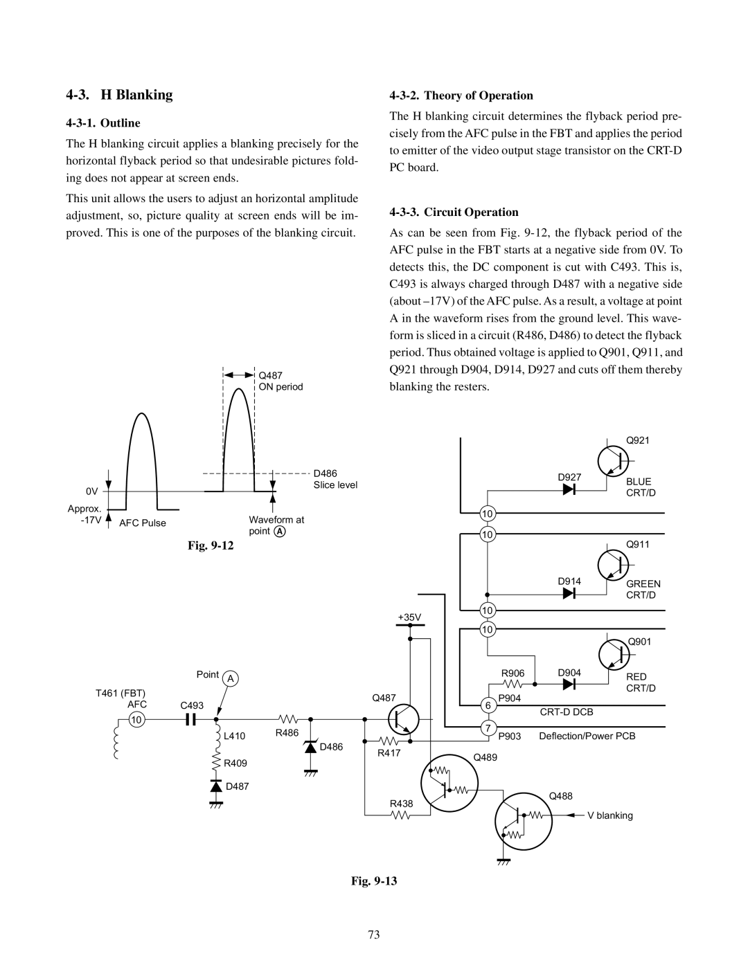
The H blanking circuit applies a blanking precisely for the horizontal flyback period so that undesirable pictures fold- ing does not appear at screen ends.
This unit allows the users to adjust an horizontal amplitude adjustment, so, picture quality at screen ends will be im- proved. This is one of the purposes of the blanking circuit.
![]()
![]() Q487
Q487
ON period
4-3-2. Theory of Operation
The H blanking circuit determines the flyback period pre- cisely from the AFC pulse in the FBT and applies the period to emitter of the video output stage transistor on the
4-3-3. Circuit Operation
As can be seen from Fig.
|
|
|
|
| D486 |
|
|
|
|
| |
0V |
|
|
|
| Slice level |
|
|
|
|
| |
Approx. |
|
|
|
|
|
| AFC Pulse | Waveform at | |||
|
|
| point | ||
Fig.
Point A
T461 (FBT)
AFC C493 10
L410 | R486 |
| |
| D486 |
R409 |
|
D487 |
|
+35V
Q487
R417
R438
Q921
D927 | BLUE |
| |
| CRT/D |
10 |
|
10 | Q911 |
| |
D914 | GREEN |
| |
| CRT/D |
10 |
|
10
Q901
| R906 | D904 | RED |
|
|
| |
|
|
| CRT/D |
6 | P904 |
| |
|
|
|
7 P903 Deflection/Power PCB
Q489
Q488
V blanking
Fig.
73