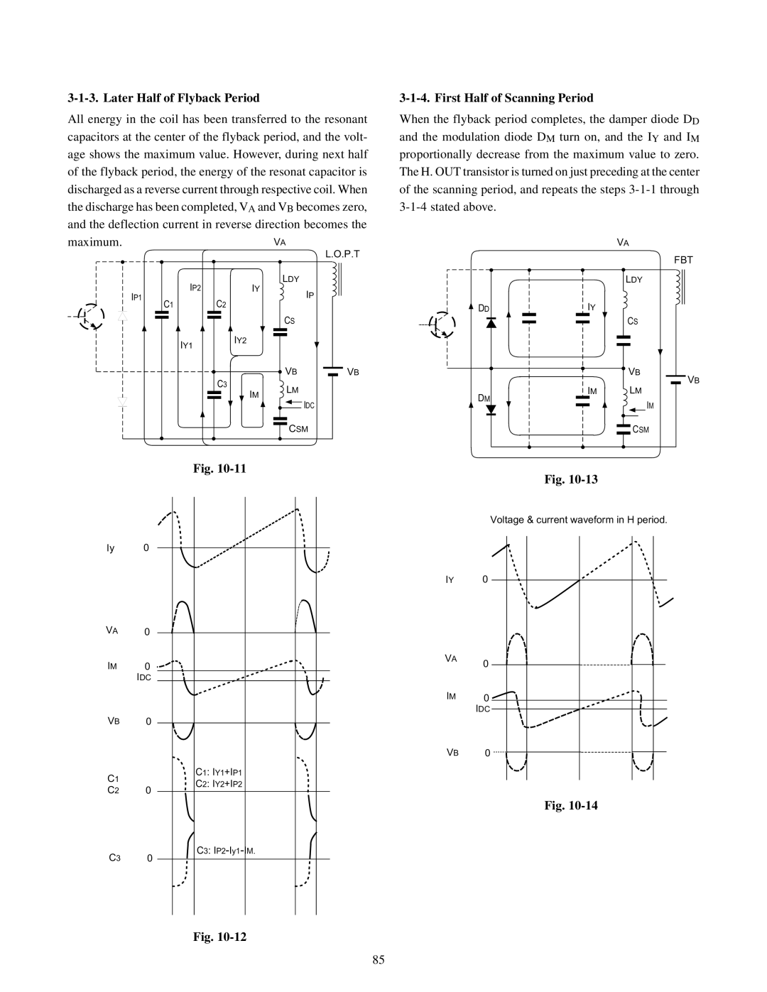
3-1-3. Later Half of Flyback Period
All energy in the coil has been transferred to the resonant capacitors at the center of the flyback period, and the volt- age shows the maximum value. However, during next half of the flyback period, the energy of the resonat capacitor is discharged as a reverse current through respective coil. When the discharge has been completed, VA and VB becomes zero, and the deflection current in reverse direction becomes the
maximum. |
|
|
| VA |
|
|
|
|
|
| L.O.P.T |
| IP2 |
| IY | LDY |
|
IP1 |
| IP |
| ||
C1 | C2 |
|
| ||
|
|
|
| ||
|
|
|
| CS |
|
| IY1 | IY2 |
|
|
|
|
|
|
|
| |
|
|
|
| VB | VB |
|
| C3 |
| LM |
|
|
|
| IM |
| |
|
|
| IDC |
| |
|
|
|
|
| |
|
|
|
| CSM |
|
| Fig. |
|
|
| |
3-1-4. First Half of Scanning Period
When the flyback period completes, the damper diode DD and the modulation diode DM turn on, and the IY and IM proportionally decrease from the maximum value to zero. The H. OUT transistor is turned on just preceding at the center of the scanning period, and repeats the steps
|
| VA |
|
| FBT |
|
| LDY |
DD | IY |
|
|
| CS |
|
| VB |
|
| VB |
DM | IM | LM |
| IM | |
|
| |
|
| CSM |
Fig.
Voltage & current waveform in H period.
Iy 0
VA 0
IM 0
IDC
VB 0
C1
C2 0
C3 0
C1: IY1+IP1
C2: IY2+IP2
![]() C3:
C3:
IY | 0 |
VA | 0 |
| |
IM | 0 |
| IDC |
VB | 0 |
| Fig. |
Fig.
85