4-3. Main/Sub Screen Superimposing Section
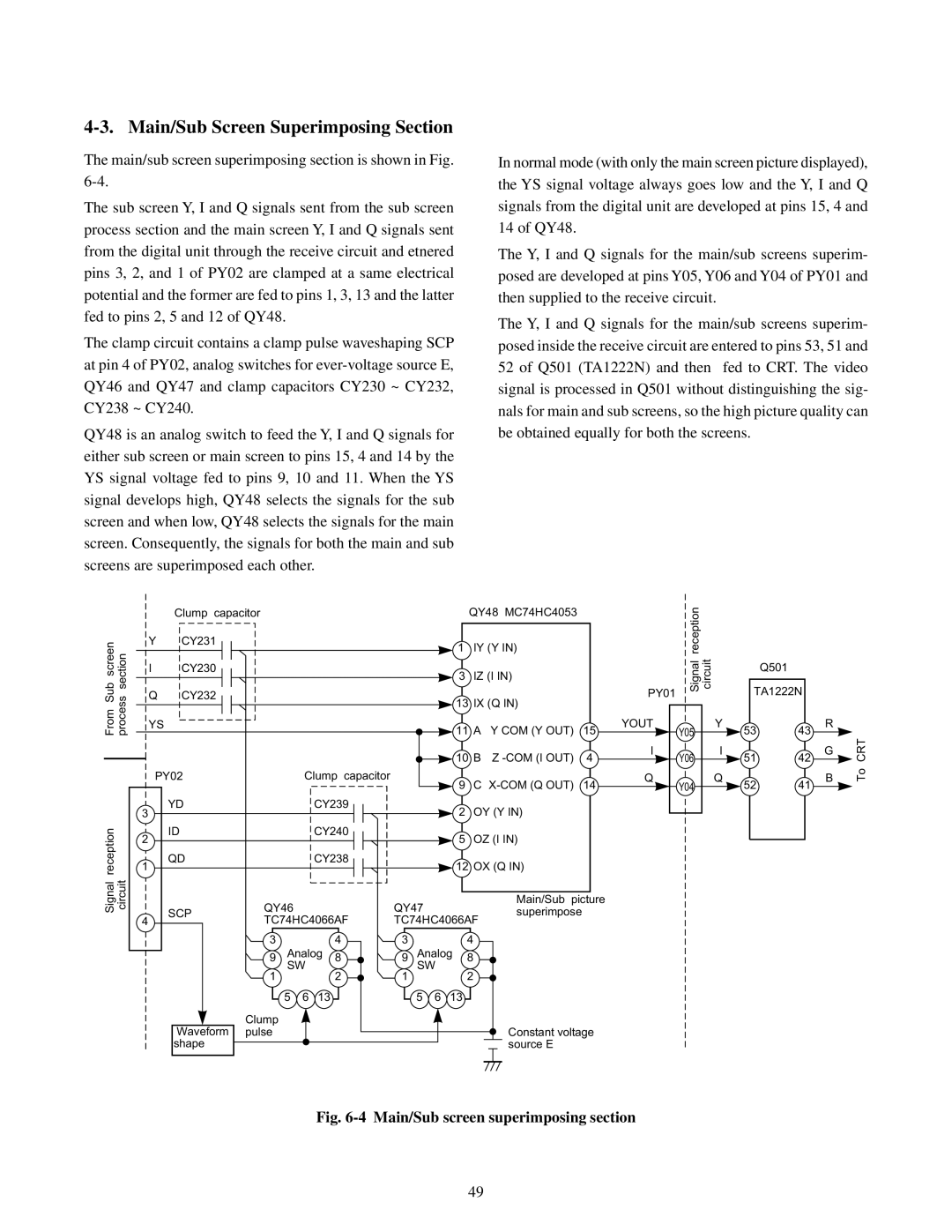
The main/sub screen superimposing section is shown in Fig.
The sub screen Y, I and Q signals sent from the sub screen process section and the main screen Y, I and Q signals sent from the digital unit through the receive circuit and etnered pins 3, 2, and 1 of PY02 are clamped at a same electrical potential and the former are fed to pins 1, 3, 13 and the latter fed to pins 2, 5 and 12 of QY48.
The clamp circuit contains a clamp pulse waveshaping SCP at pin 4 of PY02, analog switches for
QY48 is an analog switch to feed the Y, I and Q signals for either sub screen or main screen to pins 15, 4 and 14 by the YS signal voltage fed to pins 9, 10 and 11. When the YS signal develops high, QY48 selects the signals for the sub screen and when low, QY48 selects the signals for the main screen. Consequently, the signals for both the main and sub screens are superimposed each other.
In normal mode (with only the main screen picture displayed), the YS signal voltage always goes low and the Y, I and Q signals from the digital unit are developed at pins 15, 4 and 14 of QY48.
The Y, I and Q signals for the main/sub screens superim- posed are developed at pins Y05, Y06 and Y04 of PY01 and then supplied to the receive circuit.
The Y, I and Q signals for the main/sub screens superim- posed inside the receive circuit are entered to pins 53, 51 and 52 of Q501 (TA1222N) and then fed to CRT. The video signal is processed in Q501 without distinguishing the sig- nals for main and sub screens, so the high picture quality can be obtained equally for both the screens.
From Sub screen process section
Signal reception circuit
| Clump capacitor |
|
| QY48 MC74HC4053 |
| |
| Y | CY231 |
| 1 | IY (Y IN) |
|
|
|
|
|
| ||
| I | CY230 |
| 3 | IZ (I IN) |
|
|
|
|
|
| ||
| Q | CY232 |
| 13 | IX (Q IN) |
|
|
|
|
|
| ||
| YS |
|
| 11 | A Y COM (Y OUT) | 15 |
|
|
|
| |||
|
|
|
| 10 | B Z | 4 |
| PY02 | Clump capacitor | 9 | C | 14 | |
|
|
|
| |||
3 | YD | CY239 | 2 | OY (Y IN) |
| |
|
|
|
| |||
2 | ID |
| CY240 | 5 | OZ (I IN) |
|
|
|
|
| |||
1 | QD |
|
|
| CY238 |
|
|
|
| 12 OX (Q IN) |
| |||
|
|
|
|
|
|
|
|
|
|
| ||||
|
| QY46 |
|
|
| QY47 |
|
|
| Main/Sub | picture | |||
| SCP |
|
|
|
|
|
| superimpose | ||||||
4 | TC74HC4066AF | TC74HC4066AF | ||||||||||||
|
|
| ||||||||||||
|
| 3 |
|
|
| 4 | 3 |
|
|
| 4 |
|
| |
|
| 9 | Analog | 8 | 9 | Analog | 8 |
|
| |||||
|
| 1 | SW |
| 2 | 1 | SW |
| 2 |
|
| |||
|
|
|
|
|
|
|
|
|
| |||||
|
|
| 5 | 6 | 13 |
|
| 5 | 6 | 13 |
|
| ||
| Waveform | Clump |
|
|
|
|
|
|
|
|
|
|
| |
| pulse |
|
|
|
|
|
|
|
|
| Constant voltage | |||
| shape |
|
|
|
|
|
|
|
|
|
| source E |
| |
PY01 | Signal reception | circuit |
|
|
YOUT
Y05
I
Y06
Q
Y04
|
| Q501 |
|
| TA1222N |
| |
Y | 53 | 43 | R |
|
| ||
I | 51 | 42 | G |
|
| ||
Q | 52 | 41 | B |
|
| ||
To CRT
Fig. 6-4 Main/Sub screen superimposing section
49