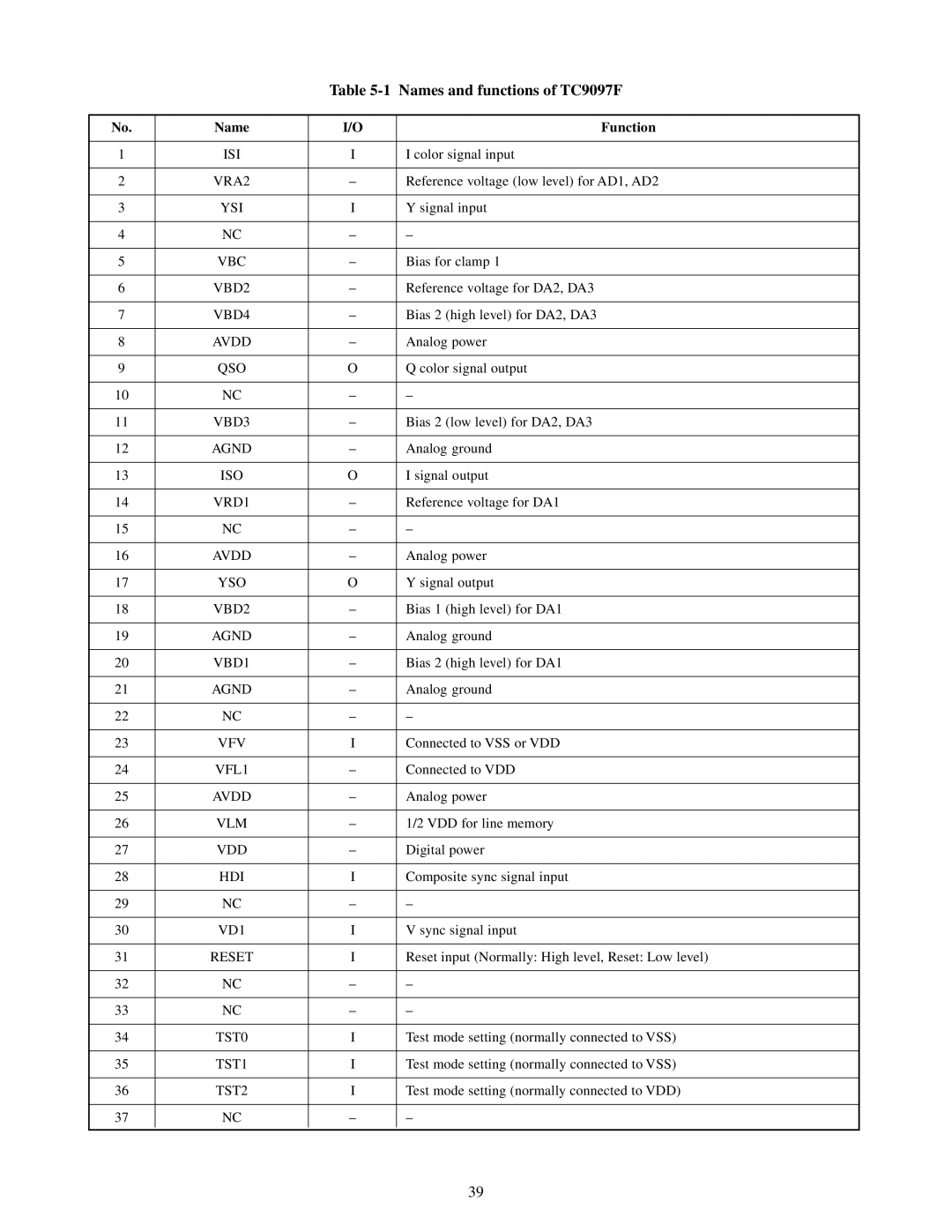
Table 5-1 Names and functions of TC9097F
No. | Name | I/O | Function |
|
|
|
|
1 | ISI | I | I color signal input |
|
|
|
|
2 | VRA2 | – | Reference voltage (low level) for AD1, AD2 |
|
|
|
|
3 | YSI | I | Y signal input |
|
|
|
|
4 | NC | – | – |
|
|
|
|
5 | VBC | – | Bias for clamp 1 |
|
|
|
|
6 | VBD2 | – | Reference voltage for DA2, DA3 |
|
|
|
|
7 | VBD4 | – | Bias 2 (high level) for DA2, DA3 |
|
|
|
|
8 | AVDD | – | Analog power |
|
|
|
|
9 | QSO | O | Q color signal output |
|
|
|
|
10 | NC | – | – |
|
|
|
|
11 | VBD3 | – | Bias 2 (low level) for DA2, DA3 |
|
|
|
|
12 | AGND | – | Analog ground |
|
|
|
|
13 | ISO | O | I signal output |
|
|
|
|
14 | VRD1 | – | Reference voltage for DA1 |
|
|
|
|
15 | NC | – | – |
|
|
|
|
16 | AVDD | – | Analog power |
|
|
|
|
17 | YSO | O | Y signal output |
|
|
|
|
18 | VBD2 | – | Bias 1 (high level) for DA1 |
|
|
|
|
19 | AGND | – | Analog ground |
|
|
|
|
20 | VBD1 | – | Bias 2 (high level) for DA1 |
|
|
|
|
21 | AGND | – | Analog ground |
|
|
|
|
22 | NC | – | – |
|
|
|
|
23 | VFV | I | Connected to VSS or VDD |
|
|
|
|
24 | VFL1 | – | Connected to VDD |
|
|
|
|
25 | AVDD | – | Analog power |
|
|
|
|
26 | VLM | – | 1/2 VDD for line memory |
|
|
|
|
27 | VDD | – | Digital power |
|
|
|
|
28 | HDI | I | Composite sync signal input |
|
|
|
|
29 | NC | – | – |
|
|
|
|
30 | VD1 | I | V sync signal input |
|
|
|
|
31 | RESET | I | Reset input (Normally: High level, Reset: Low level) |
|
|
|
|
32 | NC | – | – |
|
|
|
|
33 | NC | – | – |
|
|
|
|
34 | TST0 | I | Test mode setting (normally connected to VSS) |
|
|
|
|
35 | TST1 | I | Test mode setting (normally connected to VSS) |
|
|
|
|
36 | TST2 | I | Test mode setting (normally connected to VDD) |
|
|
|
|
37 | NC | – | – |
|
|
|
|
39