Chapter 3 |
|
|
|
|
|
| Signals and Pinout Tables | |||||
Table |
|
|
|
|
|
|
|
| ||||
|
|
|
|
|
|
|
|
|
|
|
|
|
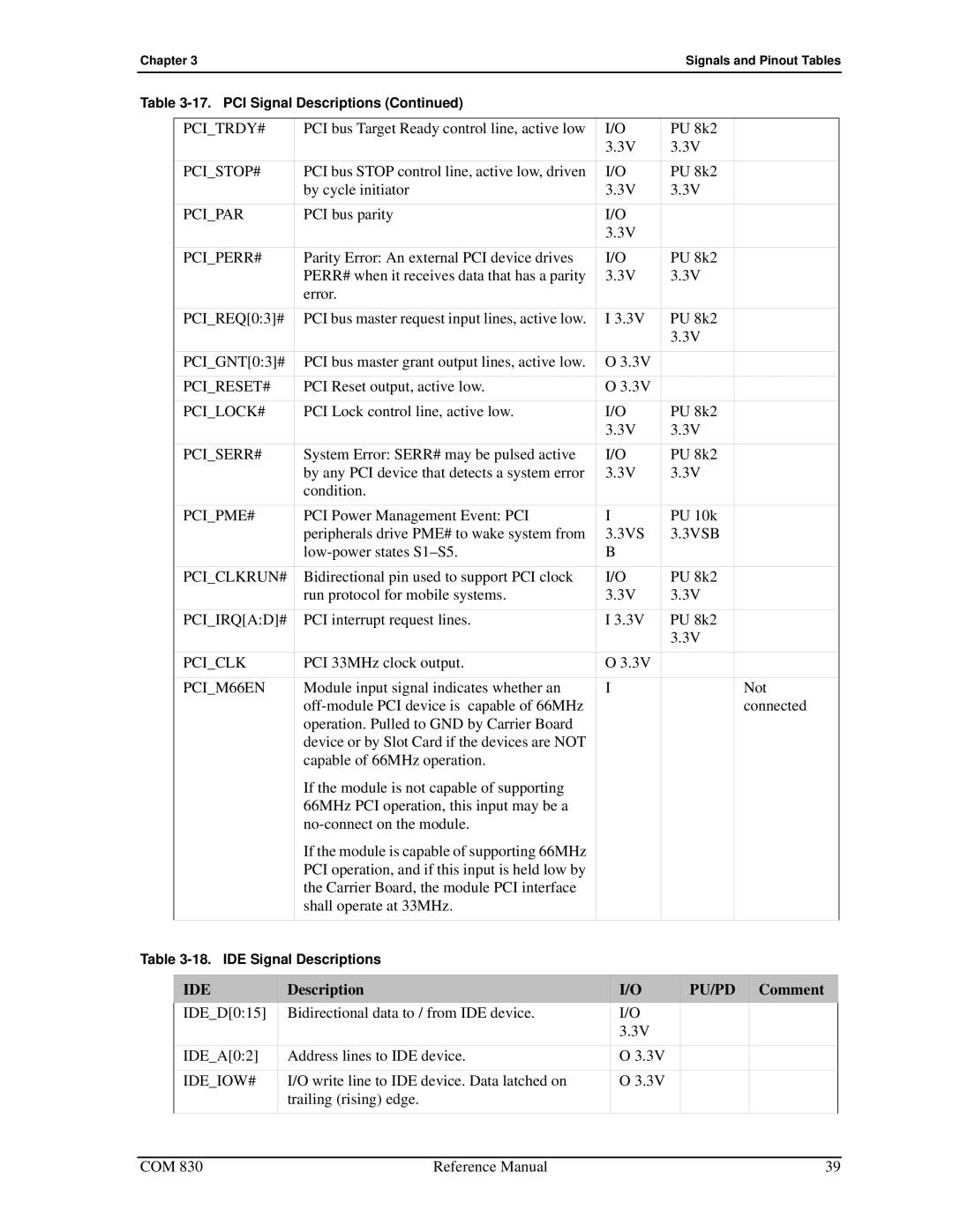
| PCI_TRDY# |
| PCI bus Target Ready control line, active low | I/O |
| PU 8k2 |
|
|
| |||
|
|
|
|
| 3.3V |
| 3.3V |
|
|
| ||
| PCI_STOP# |
| PCI bus STOP control line, active low, driven | I/O |
| PU 8k2 |
|
|
| |||
|
|
|
| by cycle initiator | 3.3V |
| 3.3V |
|
|
| ||
| PCI_PAR |
| PCI bus parity | I/O |
|
|
|
|
|
| ||
|
|
|
|
| 3.3V |
|
|
|
|
|
| |
| PCI_PERR# |
| Parity Error: An external PCI device drives | I/O |
| PU 8k2 |
|
|
| |||
|
|
|
| PERR# when it receives data that has a parity | 3.3V |
| 3.3V |
|
|
| ||
|
|
|
| error. |
|
|
|
|
|
|
|
|
| PCI_REQ[0:3]# |
| PCI bus master request input lines, active low. | I 3.3V |
| PU 8k2 |
|
|
| |||
|
|
|
|
|
|
|
| 3.3V |
|
|
| |
| PCI_GNT[0:3]# |
| PCI bus master grant output lines, active low. | O 3.3V |
|
|
|
|
|
| ||
| PCI_RESET# |
| PCI Reset output, active low. | O 3.3V |
|
|
|
|
|
| ||
| PCI_LOCK# |
| PCI Lock control line, active low. | I/O |
| PU 8k2 |
|
|
| |||
|
|
|
|
| 3.3V |
| 3.3V |
|
|
| ||
| PCI_SERR# |
| System Error: SERR# may be pulsed active | I/O |
| PU 8k2 |
|
|
| |||
|
|
|
| by any PCI device that detects a system error | 3.3V |
| 3.3V |
|
|
| ||
|
|
|
| condition. |
|
|
|
|
|
|
|
|
| PCI_PME# |
| PCI Power Management Event: PCI | I |
| PU 10k |
|
|
| |||
|
|
|
| peripherals drive PME# to wake system from | 3.3VS |
| 3.3VSB |
|
|
| ||
|
|
|
| B |
|
|
|
|
|
| ||
| PCI_CLKRUN# |
| Bidirectional pin used to support PCI clock | I/O |
| PU 8k2 |
|
|
| |||
|
|
|
| run protocol for mobile systems. | 3.3V |
| 3.3V |
|
|
| ||
| PCI_IRQ[A:D]# |
| PCI interrupt request lines. | I 3.3V |
| PU 8k2 |
|
|
| |||
|
|
|
|
|
|
|
| 3.3V |
|
|
| |
| PCI_CLK |
| PCI 33MHz clock output. | O 3.3V |
|
|
|
|
|
| ||
| PCI_M66EN |
| Module input signal indicates whether an | I |
|
|
| Not |
| |||
|
|
|
|
|
|
|
|
| connected |
| ||
|
|
|
| operation. Pulled to GND by Carrier Board |
|
|
|
|
|
|
|
|
|
|
|
| device or by Slot Card if the devices are NOT |
|
|
|
|
|
|
|
|
|
|
|
| capable of 66MHz operation. |
|
|
|
|
|
|
|
|
|
|
|
| If the module is not capable of supporting |
|
|
|
|
|
|
|
|
|
|
|
| 66MHz PCI operation, this input may be a |
|
|
|
|
|
|
|
|
|
|
|
|
|
|
|
|
|
|
|
| |
|
|
|
| If the module is capable of supporting 66MHz |
|
|
|
|
|
|
|
|
|
|
|
| PCI operation, and if this input is held low by |
|
|
|
|
|
|
|
|
|
|
|
| the Carrier Board, the module PCI interface |
|
|
|
|
|
|
|
|
|
|
|
| shall operate at 33MHz. |
|
|
|
|
|
|
|
|
|
|
|
|
|
|
|
|
|
|
|
| |
Table |
|
|
|
|
|
|
|
| ||||
|
|
|
|
|
|
|
|
|
|
|
|
|
| IDE |
| Description |
| I/O |
| PU/PD | Comment |
| |||
| IDE_D[0:15] | Bidirectional data to / from IDE device. |
| I/O |
|
|
|
|
| |||
|
|
|
|
|
| 3.3V |
|
|
|
|
| |
|
|
|
|
|
|
|
|
|
|
| ||
| IDE_A[0:2] |
| Address lines to IDE device. |
| O 3.3V |
|
|
|
|
| ||
| IDE_IOW# |
| I/O write line to IDE device. Data latched on |
| O 3.3V |
|
|
|
|
| ||
|
|
| trailing (rising) edge. |
|
|
|
|
|
|
|
| |
|
|
|
|
|
|
|
|
|
|
|
|
|
COM 830 | Reference Manual | 39 |