Chapter 3 | Signals and Pinout Tables |
CAUTION The signals listed in the table above are used as chipset configuration straps during system reset. In this condition (during reset), they are inputs that are pulled to the correct state by either COM Express internally implemented resistors or chipset internally implemented resistors that are located on the module. No external DC loads or external
AC_SYNC and AC_SDOUT can be used to switch PCI Express channels
System Resources
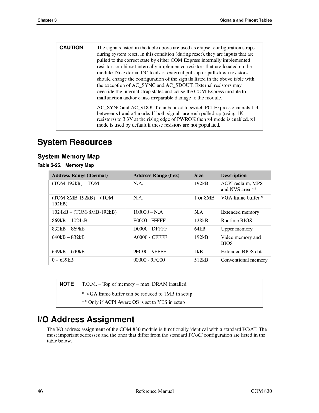
System Memory Map
Table
Address Range (decimal) | Address Range (hex) | Size | Description |
N.A. | 192kB | ACPI reclaim, MPS | |
|
|
| and NVS area ** |
N.A. | 1 or 8MB | VGA frame buffer * | |
192kB) |
|
|
|
1024kB – | 100000 – N.A | N.A. | Extended memory |
869kB – 1024kB | E0000 - FFFFF | 128kB | Runtime BIOS |
832kB – 869kB | D0000 - DFFFF | 64kB | Upper memory |
640kB – 832kB | A0000 - CFFFF | 192kB | Video memory and |
|
|
| BIOS |
639kB – 640kB | 9FC00 - 9FFFF | 1kB | Extended BIOS data |
0 – 639kB | 00000 - 9FC00 | 512kB | Conventional memory |
|
|
|
|
NOTE T.O.M. = Top of memory = max. DRAM installed
*VGA frame buffer can be reduced to 1MB in setup. ** Only if ACPI Aware OS is set to YES in setup
I/O Address Assignment
The I/O address assignment of the COM 830 module is functionally identical with a standard PC/AT. The most important addresses and the ones that differ from the standard PC/AT configuration are listed in the table below.
46 | Reference Manual | COM 830 |