Chapter 3 | Signals and Pinout Tables |
NOTE Some signals have special functionality during the reset process. They may bootstrap some basic important functions of the module.
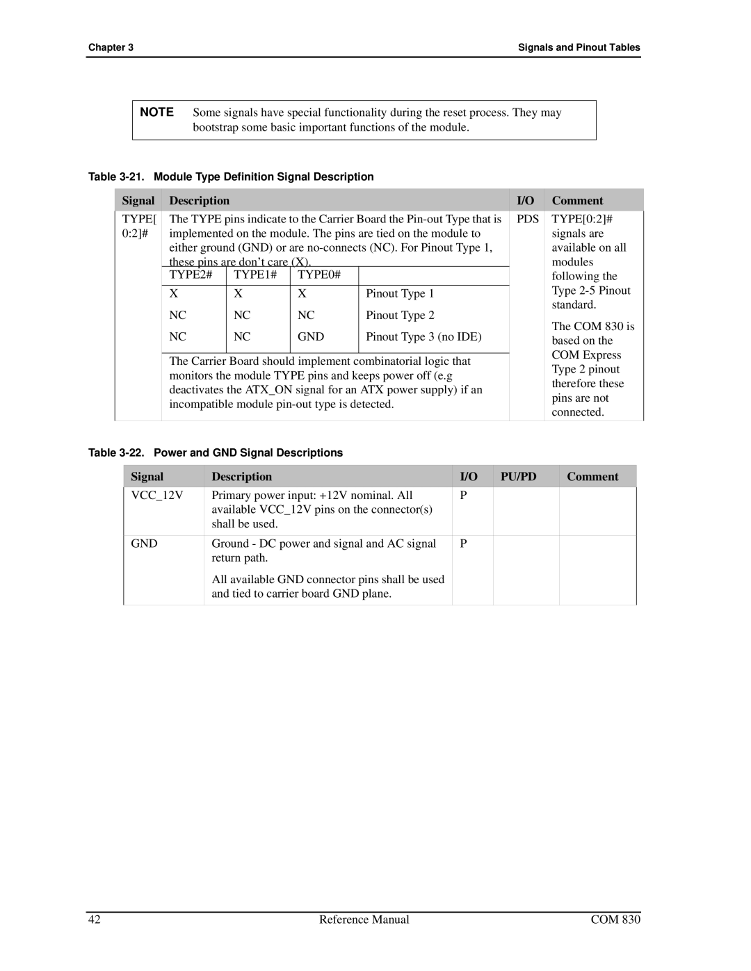
Table
| Signal |
| Description |
|
|
|
|
| I/O | Comment | |||||
| TYPE[ |
| The TYPE pins indicate to the Carrier Board the | PDS | TYPE[0:2]# | ||||||||||
| 0:2]# |
| implemented on the module. The pins are tied on the module to |
|
| signals are | |||||||||
|
|
|
| either ground (GND) or are |
|
| available on all | ||||||||
|
|
|
| these pins are don’t care (X). |
|
|
|
| modules | ||||||
|
|
|
| TYPE2# |
| TYPE1# | TYPE0# |
|
|
|
| following the | |||
|
|
|
| X |
|
| X | X | Pinout Type 1 |
|
|
| Type | ||
|
|
|
| NC |
|
| NC | NC | Pinout Type 2 |
|
|
| standard. | ||
|
|
|
|
|
|
|
|
| The COM 830 is | ||||||
|
|
|
| NC |
|
| NC | GND | Pinout Type 3 (no IDE) |
|
| ||||
|
|
|
|
|
|
|
| based on the | |||||||
|
|
|
|
|
|
|
|
|
|
|
|
| COM Express | ||
|
|
|
| The Carrier Board should implement combinatorial logic that |
|
| |||||||||
|
|
|
|
|
| Type 2 pinout | |||||||||
|
|
|
| monitors the module TYPE pins and keeps power off (e.g |
|
|
| ||||||||
|
|
|
|
|
|
| therefore these | ||||||||
|
|
|
| deactivates the ATX_ON signal for an ATX power supply) if an |
|
| |||||||||
|
|
|
|
|
| pins are not | |||||||||
|
|
|
| incompatible module |
|
|
| ||||||||
|
|
|
|
|
|
| connected. | ||||||||
|
|
|
|
|
|
|
|
|
|
|
|
| |||
|
|
|
|
|
|
|
|
|
|
|
|
|
| ||
Table |
|
|
|
|
|
|
| ||||||||
|
|
|
|
|
|
|
|
|
|
|
|
|
|
| |
|
| Signal |
| Description |
|
| I/O | PU/PD |
| Comment |
| ||||
|
| VCC_12V | Primary power input: +12V nominal. All | P |
|
|
|
|
| ||||||
|
|
|
|
| available VCC_12V pins on the connector(s) |
|
|
|
|
|
| ||||
|
|
|
|
| shall be used. |
|
|
|
|
|
|
|
| ||
|
| GND |
| Ground - DC power and signal and AC signal | P |
|
|
|
|
| |||||
|
|
|
|
| return path. |
|
|
|
|
|
|
|
| ||
|
|
|
|
| All available GND connector pins shall be used |
|
|
|
|
|
| ||||
|
|
|
|
| and tied to carrier board GND plane. |
|
|
|
|
|
| ||||
|
|
|
|
|
|
|
|
|
|
|
|
|
|
|
|
42 | Reference Manual | COM 830 |