Appendix A: Interfaces Pin Assignment
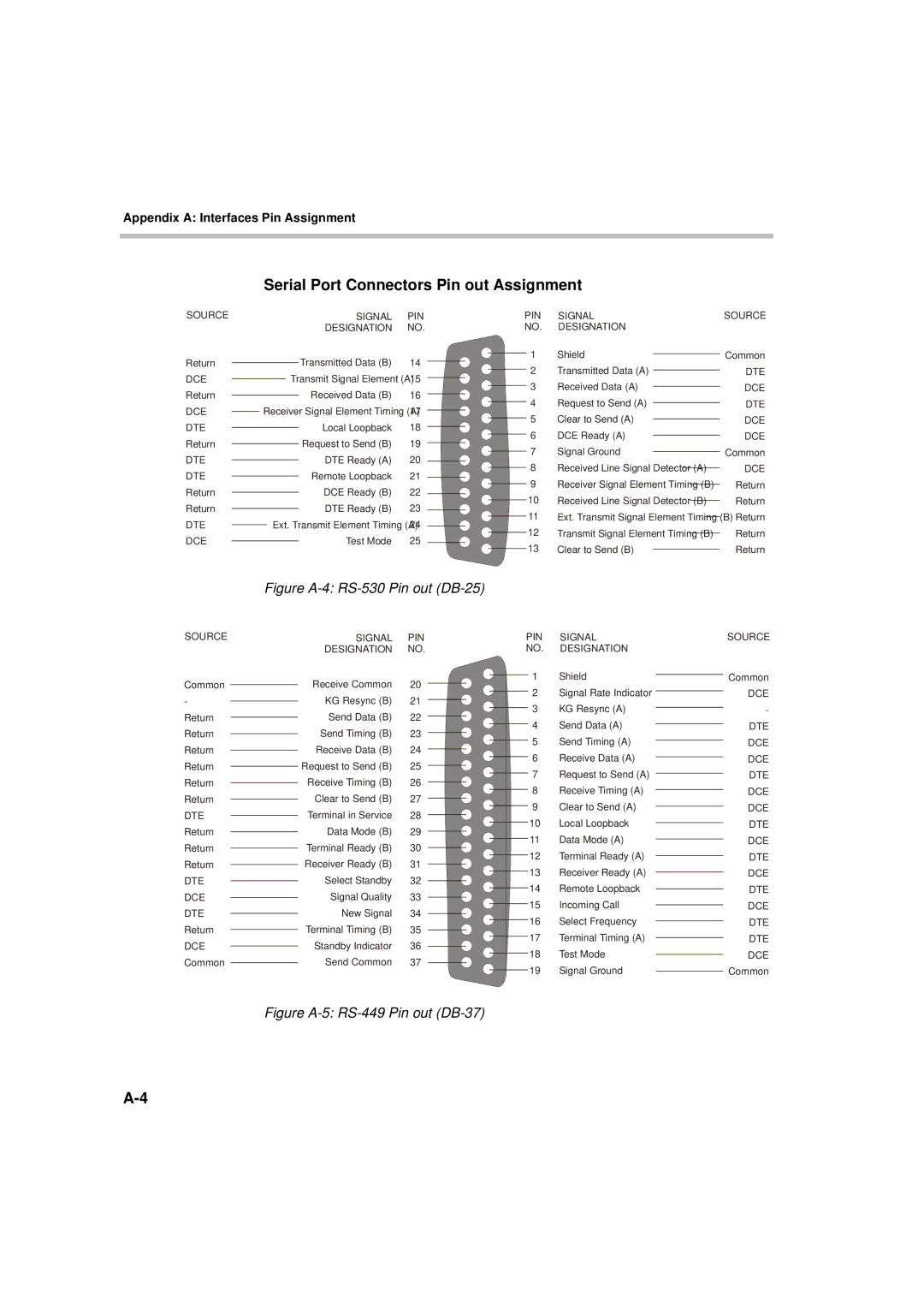
Serial Port Connectors Pin out Assignment
SOURCE |
|
|
|
| SIGNAL | PIN |
|
| PIN | SIGNAL | ||||||
|
|
|
|
| DESIGNATION | NO. |
|
| NO. | DESIGNATION | ||||||
Return |
|
|
|
| Transmitted Data (B) | 14 |
|
| 1 | Shield |
|
|
|
|
| |
|
|
|
|
|
|
|
|
|
| |||||||
|
|
|
|
|
|
| 2 | Transmitted Data (A) |
|
|
|
|
| |||
|
|
|
|
|
|
|
|
|
|
|
| |||||
DCE |
|
|
| Transmit Signal Element (A) | 15 |
|
|
|
|
|
|
| ||||
|
|
|
|
|
| 3 | Received Data (A) |
|
|
|
|
| ||||
Return |
|
|
|
| Received Data (B) | 16 |
|
|
|
|
|
|
| |||
|
|
|
|
|
|
| 4 | Request to Send (A) |
|
|
|
|
| |||
DCE |
| Receiver Signal Element Timing (A) | 17 |
|
|
|
|
|
|
| ||||||
|
|
|
| 5 | Clear to Send (A) |
|
|
|
|
| ||||||
DTE |
|
|
|
| Local Loopback | 18 |
|
|
|
|
|
|
| |||
|
|
|
|
|
|
| 6 | DCE Ready (A) |
|
|
|
|
| |||
Return |
|
|
|
| Request to Send (B) | 19 |
|
|
|
|
|
|
| |||
|
|
|
|
|
|
| 7 | Signal Ground |
|
|
|
|
| |||
DTE |
|
|
|
| DTE Ready (A) | 20 |
|
|
|
|
|
|
| |||
|
|
|
|
|
|
| 8 | Received Line Signal Detector (A) |
|
|
|
| ||||
DTE |
|
|
|
| Remote Loopback | 21 |
|
|
|
|
|
| ||||
|
|
|
|
|
|
| 9 | Receiver Signal Element Timing (B) |
|
| ||||||
Return |
|
|
|
| DCE Ready (B) | 22 |
|
|
|
| ||||||
|
|
|
|
|
|
| 10 | Received Line Signal Detector (B) |
|
| ||||||
|
|
|
|
|
|
|
|
| ||||||||
Return |
|
|
|
| DTE Ready (B) | 23 |
|
|
|
| ||||||
|
|
|
|
|
|
| 11 | Ext. Transmit Signal Element Timing (B) |
| |||||||
|
|
|
|
|
|
|
| |||||||||
DTE |
|
| Ext. Transmit Element Timing (A) | 24 |
|
|
| |||||||||
|
|
|
|
| 12 | Transmit Signal Element Timing (B) |
|
|
| |||||||
|
|
|
|
|
|
|
| |||||||||
DCE |
|
|
|
| Test Mode | 25 |
|
|
|
| ||||||
|
|
|
|
|
|
| 13 | Clear to Send (B) |
|
|
|
|
| |||
|
|
|
|
|
|
|
|
|
|
|
| |||||
|
|
|
|
|
|
|
|
|
|
| ||||||
SOURCE
Common
DTE
DCE
DTE
DCE
DCE
Common
DCE
Return
Return
Return
Return
Return
SOURCE
Common
-
Return
Return
Return
Return
Return
Return
DTE
Return
Return
Return
DTE
DCE
DTE
Return
DCE Common
Figure A-4: RS-530 Pin out (DB-25)
SIGNAL | PIN |
DESIGNATION | NO. |
Receive Common | 20 |
KG Resync (B) | 21 |
Send Data (B) | 22 |
Send Timing (B) | 23 |
Receive Data (B) | 24 |
Request to Send (B) | 25 |
Receive Timing (B) | 26 |
Clear to Send (B) | 27 |
Terminal in Service | 28 |
Data Mode (B) | 29 |
Terminal Ready (B) | 30 |
Receiver Ready (B) | 31 |
Select Standby | 32 |
Signal Quality | 33 |
New Signal | 34 |
Terminal Timing (B) | 35 |
Standby Indicator | 36 |
Send Common | 37 |
Figure A-5: RS-449 Pin out (DB-37)
PIN SIGNAL
NO. DESIGNATION
1Shield
2Signal Rate Indicator
3KG Resync (A)
4Send Data (A)
5Send Timing (A)
6Receive Data (A)
7Request to Send (A)
8Receive Timing (A)
9Clear to Send (A)
10 Local Loopback
11 Data Mode (A)
12 Terminal Ready (A)
13 Receiver Ready (A)
14 Remote Loopback
15 Incoming Call
16 Select Frequency
17 Terminal Timing (A)
18 Test Mode
19 Signal Ground
SOURCE
Common
DCE
-
DTE
DCE
DCE
DTE
DCE
DCE
DTE
DCE
DTE
DCE
DTE
DCE
DTE
DTE
DCE Common
