![]()
![]()
![]()
![]()
![]()
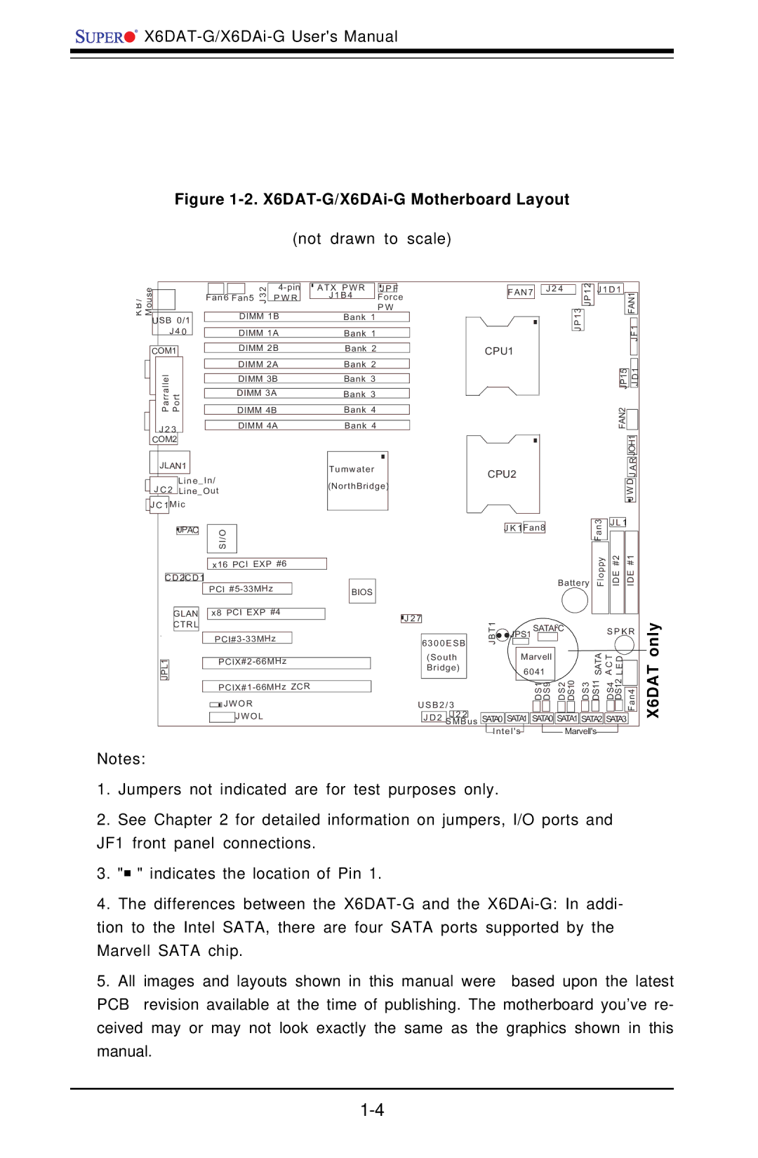
Figure 1-2. X6DAT-G/X6DAi-G Motherboard Layout
(not drawn to scale)
/Mouse
BK
USB 0/1
J 4 0
COM1
ParrallelJLAN1 Port
J 2 3
COM2
|
|
|
| 3 2 |
| ATX PWR | J P F |
| |
|
|
|
|
|
| J1B4 | Force | ||
| Fan6 |
| P W R | ||||||
| Fan5 J |
|
| ||||||
|
|
|
|
|
|
|
| P W | |
|
|
| DIMM 1B |
| Bank 1 |
|
| ||
|
|
|
|
|
|
|
|
|
|
|
|
| DIMM 1A |
| Bank 1 |
|
| ||
|
|
|
|
|
|
|
|
|
|
|
|
| DIMM 2B |
| Bank 2 |
|
| ||
|
|
|
|
|
|
|
|
|
|
|
|
| DIMM 2A |
| Bank 2 |
|
| ||
|
|
|
|
|
|
|
|
|
|
|
|
| DIMM 3B |
| Bank 3 |
|
| ||
|
|
|
|
|
|
|
|
|
|
|
|
| DIMM 3A |
| Bank 3 |
|
| ||
|
|
|
|
|
|
|
|
|
|
|
|
| DIMM 4B |
| Bank 4 |
|
| ||
|
|
|
|
|
|
|
|
|
|
|
|
| DIMM 4A |
| Bank 4 |
|
| ||
| FAN7 |
| J 2 4 |
| JP12 |
| J1D1 |
|
|
|
| |
|
|
|
|
|
|
|
|
|
| FAN1 | ||
|
|
|
|
|
|
|
|
| ||||
|
|
|
| JP13 |
|
|
|
|
|
| F1 | |
|
|
|
|
|
|
|
|
|
|
| ||
|
|
|
|
|
|
|
|
|
|
| J | |
CPU1 |
|
|
|
|
|
|
|
|
|
| ||
|
|
|
|
|
|
|
|
|
|
| 1 | |
|
|
|
|
|
|
|
| JP15 |
|
| D | |
|
|
|
|
|
|
|
|
|
| J | ||
|
|
|
|
|
|
| FAN2 |
|
|
|
| |
|
|
|
|
|
|
|
|
|
|
| ||
|
|
|
|
|
|
|
|
|
|
|
|
|
|
|
|
|
|
|
|
|
|
| JOH1 | ||
|
|
|
|
|
|
|
|
|
| R |
| |
JLAN1 |
| Tumwater | |||
|
| Line_In/ | (NorthBridge) | ||
J C 2 | |||||
Line_Out | |||||
| |||||
|
|
| |||
J C 1 | Mic |
| |||
|
|
|
|
| |
CPU2 | A |
J | |
| |
| J WD |
| JPAC |
| SI/O |
|
|
|
|
|
|
|
|
| |
|
|
|
|
|
| |
|
|
| x16 PCI EXP #6 |
| ||
|
|
|
|
|
|
|
C D 2C D 1 |
|
|
|
|
| |
|
|
|
|
|
| |
|
|
| PCI |
|
| |
|
|
|
|
| ||
| GLAN |
| x8 PCI EXP #4 |
| ||
| CTRL |
|
|
|
|
|
|
|
|
|
| ||
BIOS
![]()
![]()
![]() J 2 7
J 2 7
6300ESB
| J K 1Fan8 | Fan3 | J L 1 |
|
|
|
| ||
|
|
|
| |
| Battery | Floppy | IDE #2 | IDE #1 |
T1 | SATAI2C |
| S P K R | |
JB | JPS1 |
|
|
|
|
|
|
| |
only
JPL1 |
|
| ||
|
|
|
| |
|
|
| ||
|
|
| JW OR | |
|
|
|
| JW OL |
|
|
|
| |
|
|
|
|
|
|
|
|
| 6041 |
|
|
|
|
|
|
|
| SATA CAT ELD |
| |||||||||||||
| (South |
|
| Marvell |
|
|
|
|
|
|
|
|
|
|
|
|
|
|
|
| ||||||||||||
| Bridge) |
|
|
|
|
|
|
|
|
|
|
|
|
|
|
|
|
|
|
|
|
|
|
|
|
|
| |||||
|
|
|
|
|
|
|
|
|
|
|
|
|
|
|
|
| DS2 DS10 | DS3 |
| DS11 DS4 | DS12 |
|
|
| ||||||||
|
|
|
|
|
|
|
|
|
|
|
|
|
|
|
|
|
|
|
|
| ||||||||||||
|
|
|
|
|
|
|
|
|
|
|
| DS1 DS9 |
| |||||||||||||||||||
|
|
|
|
|
|
|
|
|
|
|
|
|
|
| ||||||||||||||||||
USB2/3 |
|
|
| Fan4 | ||||||||||||||||||||||||||||
|
|
|
|
|
|
|
|
|
| |||||||||||||||||||||||
|
|
|
|
|
|
|
|
|
|
|
|
|
|
|
|
|
|
|
|
|
|
|
|
| ||||||||
| J D 2 | J 2 2 |
| SATA0 | SATA1 | SATA0 | SATA1 | SATA2 | SATA3 |
| ||||||||||||||||||||||
| SMBus |
| ||||||||||||||||||||||||||||||
|
|
| ||||||||||||||||||||||||||||||
|
|
|
|
|
| Intel's |
|
|
|
|
|
|
|
|
| Marvell's |
|
|
|
|
|
|
| |||||||||
X6DAT
Notes:
1.Jumpers not indicated are for test purposes only.
2.See Chapter 2 for detailed information on jumpers, I/O ports and JF1 front panel connections.
3."![]() " indicates the location of Pin 1.
" indicates the location of Pin 1.
4.The differences between the
5.All images and layouts shown in this manual were based upon the latest PCB revision available at the time of publishing. The motherboard you’ve re- ceived may or may not look exactly the same as the graphics shown in this manual.