|
|
|
|
|
|
|
|
|
|
|
|
|
|
| CY7C65113C | ||||
|
|
|
|
|
|
|
|
|
|
|
|
|
|
|
|
|
|
|
|
Table |
|
|
|
|
|
|
|
|
|
|
| ||||||||
|
|
|
|
|
|
|
|
|
|
|
|
|
|
| |||||
|
|
|
|
|
|
| USB Status And Control Register (0x1F) Bits [7, 6] |
|
|
|
|
|
|
| |||||
| [0,0] |
|
|
|
| [1,0] |
|
| [0,1] |
|
|
| [1,1] |
|
|
| |||
Two USB Addresses: | Two USB Addresses: | One USB Address: |
| One USB Address: |
|
| |||||||||||||
A (3 Endpoints) and | A (3 Endpoints) and |
|
|
| |||||||||||||||
| B (2 Endpoints) |
|
|
| B (2 Endpoints) |
| A (5 Endpoints) |
| A (5 Endpoints) |
|
| ||||||||
Label |
| Start Address | Size | Label | Start Address | Size | Label | Start Address |
| Size | Label |
| Start Address | Size | |||||
EPB1 |
|
| 0xD8 | 8 |
| EPB0 | 0xA8 | 8 | EPA4 | 0xD8 |
| 8 | EPA3 |
| 0xA8 |
| 8 |
| |
|
|
|
|
|
|
|
|
|
|
|
|
|
|
|
|
|
|
| |
EPB0 |
|
| 0xE0 | 8 |
| EPB1 | 0xB0 | 8 | EPA3 | 0xE0 |
| 8 | EPA4 |
| 0xB0 |
| 8 |
| |
|
|
|
|
|
|
|
|
|
|
|
|
|
|
|
|
|
|
| |
EPA2 |
|
| 0xE8 | 8 |
| EPA0 | 0xB8 | 8 | EPA2 | 0xE8 |
| 8 | EPA0 |
| 0xB8 |
| 8 |
| |
|
|
|
|
|
|
|
|
|
|
|
|
|
|
|
|
|
|
| |
EPA1 |
|
| 0xF0 | 8 |
| EPA1 | 0xC0 | 32 | EPA1 | 0xF0 |
| 8 | EPA1 |
| 0xC0 |
| 32 |
| |
|
|
|
|
|
|
|
|
|
|
|
|
|
|
|
|
|
|
| |
EPA0 |
|
| 0xF8 | 8 |
| EPA2 | 0xE0 | 32 | EPA0 | 0xF8 |
| 8 | EPA2 |
| 0xE0 |
| 32 |
| |
When the SIE writes data to a FIFO, the internal data bus is driven by the SIE; not the CPU. This causes a short delay in the CPU operation. The delay is three clock cycles per byte. For example, an
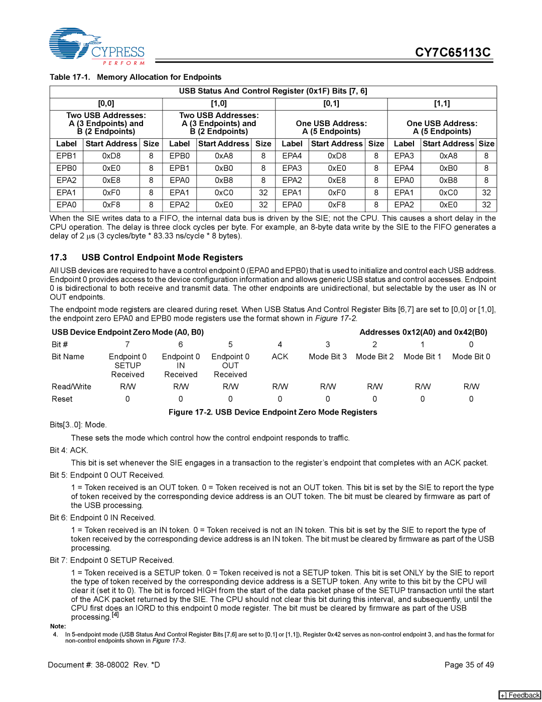
17.3USB Control Endpoint Mode Registers
All USB devices are required to have a control endpoint 0 (EPA0 and EPB0) that is used to initialize and control each USB address. Endpoint 0 provides access to the device configuration information and allows generic USB status and control accesses. Endpoint 0 is bidirectional to both receive and transmit data. The other endpoints are unidirectional, but selectable by the user as IN or OUT endpoints.
The endpoint mode registers are cleared during reset. When USB Status And Control Register Bits [6,7] are set to [0,0] or [1,0], the endpoint zero EPA0 and EPB0 mode registers use the format shown in Figure
USB Device Endpoint Zero Mode (A0, B0) |
|
|
| Addresses 0x12(A0) and 0x42(B0) | ||||
Bit # | 7 | 6 | 5 | 4 | 3 | 2 | 1 | 0 |
Bit Name | Endpoint 0 | Endpoint 0 | Endpoint 0 | ACK | Mode Bit 3 | Mode Bit 2 | Mode Bit 1 | Mode Bit 0 |
| SETUP | IN | OUT |
|
|
|
|
|
| Received | Received | Received |
|
|
|
|
|
Read/Write | R/W | R/W | R/W | R/W | R/W | R/W | R/W | R/W |
Reset | 0 | 0 | 0 | 0 | 0 | 0 | 0 | 0 |
Figure 17-2. USB Device Endpoint Zero Mode Registers
Bits[3..0]: Mode.
These sets the mode which control how the control endpoint responds to traffic. Bit 4: ACK.
This bit is set whenever the SIE engages in a transaction to the register’s endpoint that completes with an ACK packet. Bit 5: Endpoint 0 OUT Received.
1 = Token received is an OUT token. 0 = Token received is not an OUT token. This bit is set by the SIE to report the type of token received by the corresponding device address is an OUT token. The bit must be cleared by firmware as part of the USB processing.
Bit 6: Endpoint 0 IN Received.
1 = Token received is an IN token. 0 = Token received is not an IN token. This bit is set by the SIE to report the type of token received by the corresponding device address is an IN token. The bit must be cleared by firmware as part of the USB processing.
Bit 7: Endpoint 0 SETUP Received.
1 = Token received is a SETUP token. 0 = Token received is not a SETUP token. This bit is set ONLY by the SIE to report the type of token received by the corresponding device address is a SETUP token. Any write to this bit by the CPU will clear it (set it to 0). The bit is forced HIGH from the start of the data packet phase of the SETUP transaction until the start of the ACK packet returned by the SIE. The CPU should not clear this bit during this interval, and subsequently, until the CPU first does an IORD to this endpoint 0 mode register. The bit must be cleared by firmware as part of the USB processing.[4]
Note:
4.In
Document #: | Page 35 of 49 |
[+] Feedback