|
|
|
|
| CY7C65113C | |
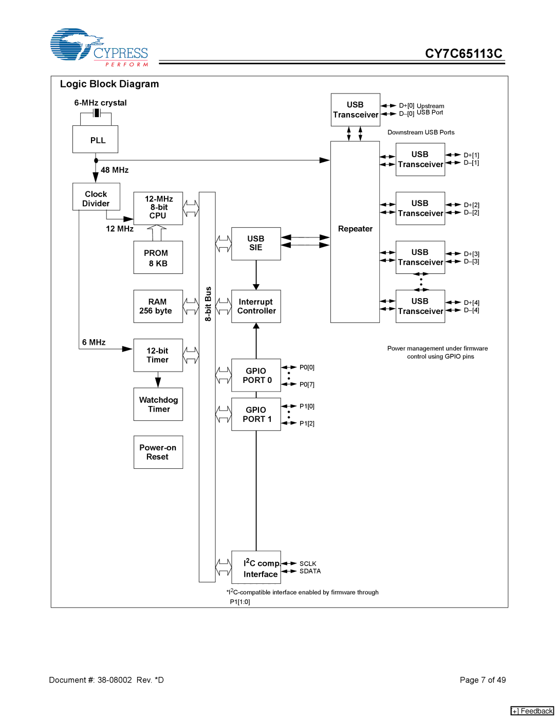
Logic Block Diagram |
|
|
|
|
| |
|
|
| USB | D+[0] Upstream |
| |
|
|
|
| Transceiver |
| |
PLL |
|
|
|
| Downstream USB Ports |
|
|
|
|
|
|
| |
|
|
|
|
| USB | D+[1] |
48 MHz |
|
|
|
| Transceiver | |
|
|
|
|
|
| |
Clock |
|
|
| USB |
| |
Divider |
|
|
| D+[2] | ||
|
|
| ||||
|
|
|
| Transceiver | ||
| CPU |
|
|
| ||
|
|
|
|
| ||
12 MHz |
|
| USB | Repeater |
|
|
|
|
|
|
|
| |
| PROM |
| SIE |
| USB | D+[3] |
|
|
|
| |||
| 8 KB |
|
|
| Transceiver | |
| RAM | Bus | Interrupt |
| USB | D+[4] |
|
| |||||
| 256 byte | Controller |
| Transceiver | ||
|
| 8 |
|
|
|
|
6 MHz |
|
|
| Power management under firmware | ||
|
|
|
| |||
| Timer |
|
|
| control using GPIO pins | |
|
|
| P0[0] |
|
| |
|
|
| GPIO |
|
| |
|
|
|
|
|
| |
|
|
| PORT 0 | P0[7] |
|
|
|
|
|
|
|
| |
| Watchdog |
|
| P1[0] |
|
|
| Timer |
| GPIO |
|
| |
|
|
|
|
| ||
|
|
| PORT 1 | P1[2] |
|
|
|
|
|
|
|
| |
|
|
|
|
|
| |
| Reset |
|
|
|
|
|
|
|
| I2C comp. | SCLK |
|
|
|
|
| Interface | SDATA |
|
|
|
|
|
|
|
| |
|
|
|
|
| ||
|
|
| P1[1:0] |
|
|
|
Document #: |
|
|
|
| Page 7 of 49 | |
[+] Feedback
