CY7C65113C
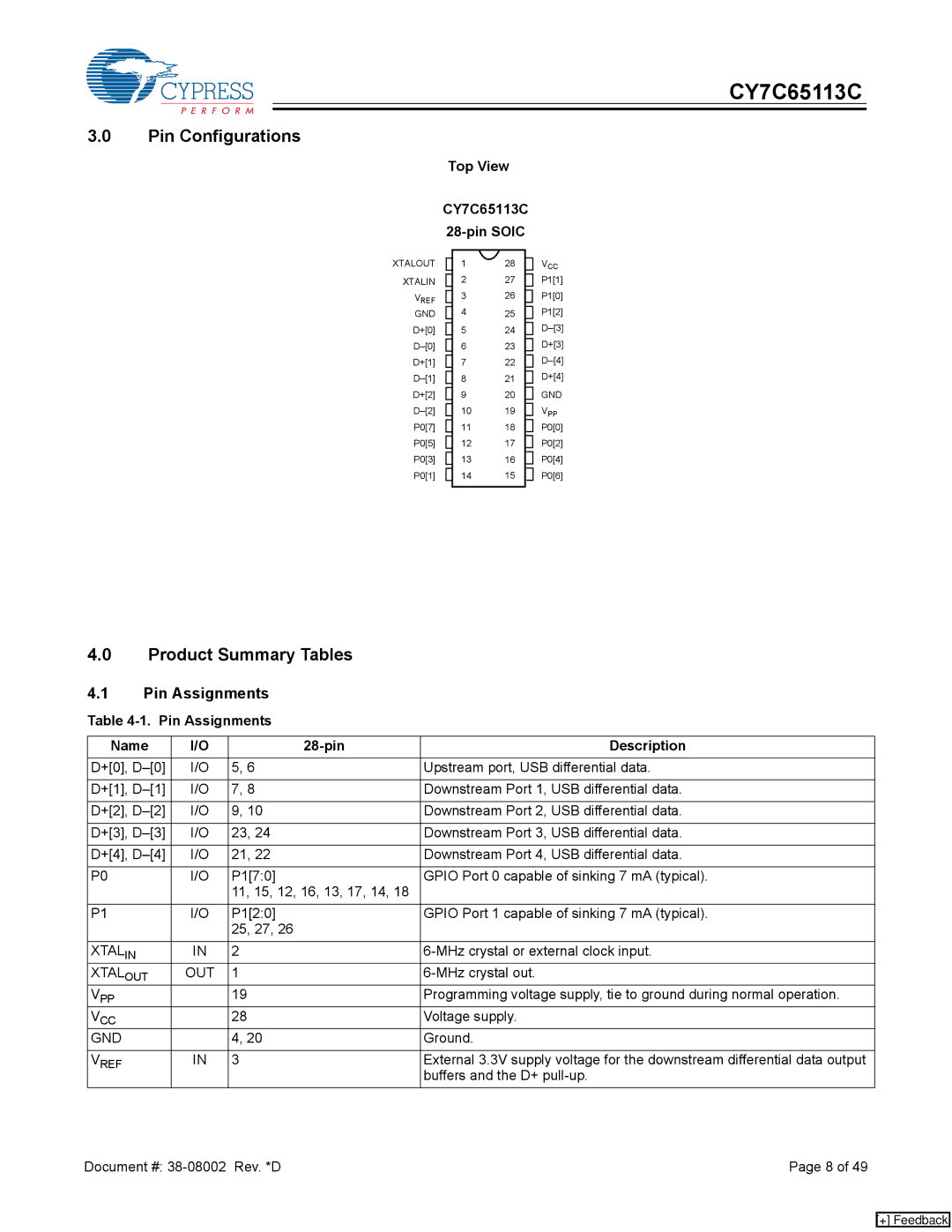
3.0Pin Configurations
Top View
CY7C65113C 28-pin SOIC
XTALOUT
XTALIN
VREF
GND
D+[0]
D+[1]
D+[2]
P0[7]
P0[5]
P0[3]
P0[1]
128
227
326
425
524
623
722
821
920
1019
1118
1217
1316
1415
VCC
P1[1]
P1[0]
P1[2]
D+[3]
D+[4]
GND
VPP
P0[0]
P0[2]
P0[4]
P0[6]
4.0Product Summary Tables
4.1Pin Assignments
Table 4-1. Pin Assignments
Name | I/O |
| Description |
D+[0], | I/O | 5, 6 | Upstream port, USB differential data. |
|
|
|
|
D+[1], | I/O | 7, 8 | Downstream Port 1, USB differential data. |
|
|
|
|
D+[2], | I/O | 9, 10 | Downstream Port 2, USB differential data. |
|
|
|
|
D+[3], | I/O | 23, 24 | Downstream Port 3, USB differential data. |
|
|
|
|
D+[4], | I/O | 21, 22 | Downstream Port 4, USB differential data. |
|
|
|
|
P0 | I/O | P1[7:0] | GPIO Port 0 capable of sinking 7 mA (typical). |
|
| 11, 15, 12, 16, 13, 17, 14, 18 |
|
P1 | I/O | P1[2:0] | GPIO Port 1 capable of sinking 7 mA (typical). |
|
| 25, 27, 26 |
|
XTALIN | IN | 2 | |
XTALOUT | OUT | 1 | |
VPP |
| 19 | Programming voltage supply, tie to ground during normal operation. |
VCC |
| 28 | Voltage supply. |
GND |
| 4, 20 | Ground. |
|
|
|
|
VREF | IN | 3 | External 3.3V supply voltage for the downstream differential data output |
|
|
| buffers and the D+ |
Document #: | Page 8 of 49 |
[+] Feedback