CY7C65113C
6.0Clocking
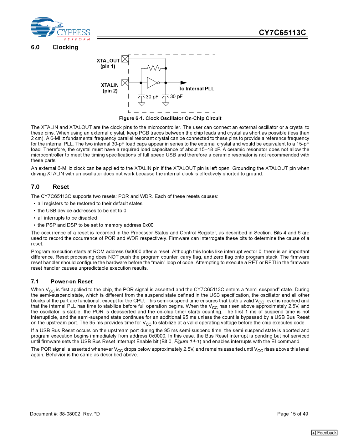
XTALOUT |
| |
(pin 1) |
| |
XTALIN | To Internal PLL | |
(pin 2) | ||
30 pF | ||
30 pF |
Figure 6-1. Clock Oscillator On-Chip Circuit
The XTALIN and XTALOUT are the clock pins to the microcontroller. The user can connect an external oscillator or a crystal to these pins. When using an external crystal, keep PCB traces between the chip leads and crystal as short as possible (less than 2 cm). A
An external
7.0Reset
The CY7C65113C supports two resets: POR and WDR. Each of these resets causes:
•all registers to be restored to their default states
•the USB device addresses to be set to 0
•all interrupts to be disabled
•the PSP and DSP to be set to memory address 0x00.
The occurrence of a reset is recorded in the Processor Status and Control Register, as described in Section. Bits 4 and 6 are used to record the occurrence of POR and WDR respectively. Firmware can interrogate these bits to determine the cause of a reset.
Program execution starts at ROM address 0x0000 after a reset. Although this looks like interrupt vector 0, there is an important difference. Reset processing does NOT push the program counter, carry flag, and zero flag onto program stack. The firmware reset handler should configure the hardware before the “main” loop of code. Attempting to execute a RET or RETI in the firmware reset handler causes unpredictable execution results.
7.1Power-on Reset
When VCC is first applied to the chip, the POR signal is asserted and the CY7C65113C enters a
If a USB Bus Reset occurs on the upstream port during the 95 ms
The POR signal is asserted whenever VCC drops below approximately 2.5V, and remains asserted until VCC rises above this level again. Behavior is the same as described above.
Document #: | Page 15 of 49 |
[+] Feedback