CY7C65113C
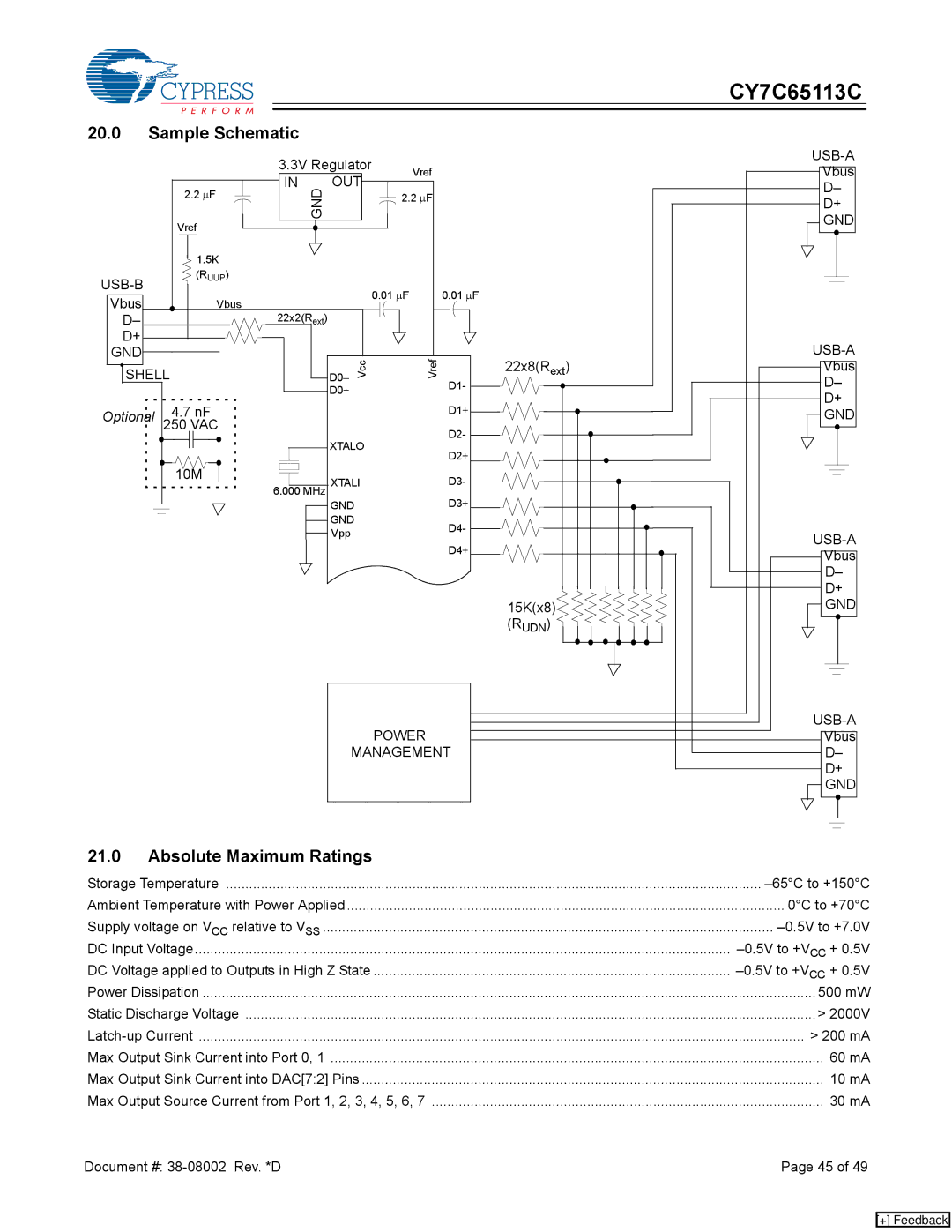
20.0Sample Schematic
|
|
| 3.3V Regulator |
|
| |||
|
|
| Vref |
| Vbus | |||
|
|
| IN | OUT |
| |||
|
|
|
|
| D– | |||
|
| 2.2 ∝F | GND |
|
| 2.2 ∝F |
| |
|
|
|
|
| D+ | |||
|
|
|
|
|
|
| ||
|
| Vref |
|
|
|
| GND | |
|
|
|
|
|
|
| ||
|
|
|
|
|
|
|
| |
|
| 1.5K |
|
|
|
|
|
|
| (RUUP) |
|
|
|
|
|
| |
|
|
|
| 0.01 | ∝F | 0.01 ∝F |
| |
Vbus |
| Vbus |
|
|
| |||
|
|
|
|
|
|
| ||
D– |
|
| 22x2(Rext) |
|
|
|
|
|
D+ |
|
|
|
|
|
|
| |
GND |
|
|
|
|
| Vref |
| |
SHELL |
|
| D0– | Vcc | 22x8(Rext) | Vbus | ||
|
|
|
| D1- | D– | |||
|
|
|
| D0+ |
|
| ||
|
|
|
|
|
|
| D+ | |
|
| 4.7 nF |
|
|
|
| D1+ | |
Optional |
|
|
|
|
| GND | ||
250 VAC |
|
|
|
| D2- |
| ||
|
|
|
| XTALO |
|
| ||
|
|
|
|
| D2+ |
| ||
|
|
|
|
|
|
|
| |
|
| 10M | 6.000 MHz XTALI |
| D3- |
| ||
|
|
|
|
| ||||
|
|
|
| D3+ |
| |||
|
|
|
| GND |
|
|
| |
|
|
|
| GND |
|
| D4- |
|
|
|
|
| Vpp |
|
| ||
|
|
|
|
|
|
| ||
|
|
|
|
|
|
| D4+ | |
|
|
|
|
|
|
| Vbus | |
|
|
|
|
|
|
|
| D– |
|
|
|
|
|
|
|
| D+ |
|
|
|
|
|
|
| 15K(x8) | GND |
|
|
|
|
|
|
| (RUDN) |
|
|
|
|
|
| POWER |
| ||
|
|
|
|
|
| Vbus | ||
|
|
|
| MANAGEMENT | D– | |||
|
|
|
|
|
|
|
| D+ |
|
|
|
|
|
|
|
| GND |
21.0Absolute Maximum Ratings
Storage Temperature | |
Ambient Temperature with Power Applied | 0°C to +70°C |
Supply voltage on VCC relative to VSS | |
DC Input Voltage | |
DC Voltage applied to Outputs in High Z State | |
Power Dissipation | 500 mW |
Static Discharge Voltage | > 2000V |
> 200 mA | |
Max Output Sink Current into Port 0, 1 | 60 mA |
Max Output Sink Current into DAC[7:2] Pins | 10 mA |
Max Output Source Current from Port 1, 2, 3, 4, 5, 6, 7 | 30 mA |
Document #: | Page 45 of 49 |
[+] Feedback