CY7C65113C
22.0Electrical Characteristics
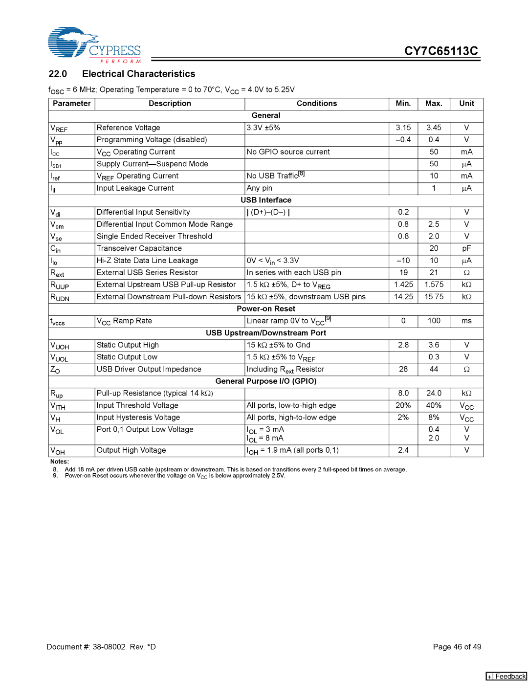
fOSC = 6 MHz; Operating Temperature = 0 to 70°C, VCC = 4.0V to 5.25V
Parameter | Description |
| Conditions | Min. | Max. | Unit |
|
| General |
|
|
| |
|
|
|
|
|
| |
VREF | Reference Voltage | 3.3V ±5% | 3.15 | 3.45 | V | |
Vpp | Programming Voltage (disabled) |
|
| 0.4 | V | |
ICC | VCC Operating Current | No GPIO source current |
| 50 | mA | |
ISB1 | Supply |
|
|
| 50 | ∝A |
Iref | VREF Operating Current | No USB Traffic[8] |
| 10 | mA | |
Iil | Input Leakage Current | Any pin |
| 1 | ∝A | |
|
| USB Interface |
|
|
| |
|
|
|
|
|
| |
Vdi | Differential Input Sensitivity | 0.2 |
| V | ||
Vcm | Differential Input Common Mode Range |
|
| 0.8 | 2.5 | V |
Vse | Single Ended Receiver Threshold |
|
| 0.8 | 2.0 | V |
Cin | Transceiver Capacitance |
|
|
| 20 | pF |
Ilo | 0V < Vin < 3.3V | 10 | ∝A | |||
Rext | External USB Series Resistor | In series with each USB pin | 19 | 21 | Ω | |
RUUP | External Upstream USB | 1.5 kΩ ±5%, D+ to VREG | 1.425 | 1.575 | kΩ | |
RUDN | External Downstream | 15 kΩ ±5%, downstream USB pins | 14.25 | 15.75 | kΩ | |
|
|
|
| |||
|
|
|
|
|
| |
tvccs | VCC Ramp Rate | Linear ramp 0V to VCC[9] | 0 | 100 | ms | |
| USB | Upstream/Downstream Port |
|
|
| |
|
|
|
|
|
| |
VUOH | Static Output High | 15 kΩ ±5% to Gnd | 2.8 | 3.6 | V | |
VUOL | Static Output Low | 1.5 kΩ ±5% to VREF |
| 0.3 | V | |
ZO | USB Driver Output Impedance | Including Rext Resistor | 28 | 44 | Ω | |
| General | Purpose I/O (GPIO) |
|
|
| |
|
|
|
|
|
|
|
Rup |
|
| 8.0 | 24.0 | kΩ | |
VITH | Input Threshold Voltage | All ports, | 20% | 40% | VCC | |
VH | Input Hysteresis Voltage | All ports, | 2% | 8% | VCC | |
VOL | Port 0,1 Output Low Voltage | IOL | = 3 mA |
| 0.4 | V |
|
| IOL | = 8 mA |
| 2.0 | V |
VOH | Output High Voltage | IOH = 1.9 mA (all ports 0,1) | 2.4 |
| V | |
Notes:
8.Add 18 mA per driven USB cable (upstream or downstream. This is based on transitions every 2
9.
Document #: | Page 46 of 49 |
[+] Feedback