CY7C65113C
9.0General-purpose I/O Ports
GPIO |
| |
CFG |
| |
OE |
| |
Internal | Data | |
Data Bus | Out | |
| Latch | |
Port Write |
| |
Port Read | Data | |
In | ||
| ||
| Latch | |
Reg_Bit |
| |
STRB |
| |
(Latch is Transparent) |
| |
| Data | |
| Interrupt | |
| Latch | |
Interrupt |
| |
Enable |
|
Interrupt
Controller
VCC
mode
| Q1 | Q2 |
Control | 14 kΩ | GPIO |
|
| |
|
| PIN |
| Q3* |
|
Control
*Port 0,1: Low Isink
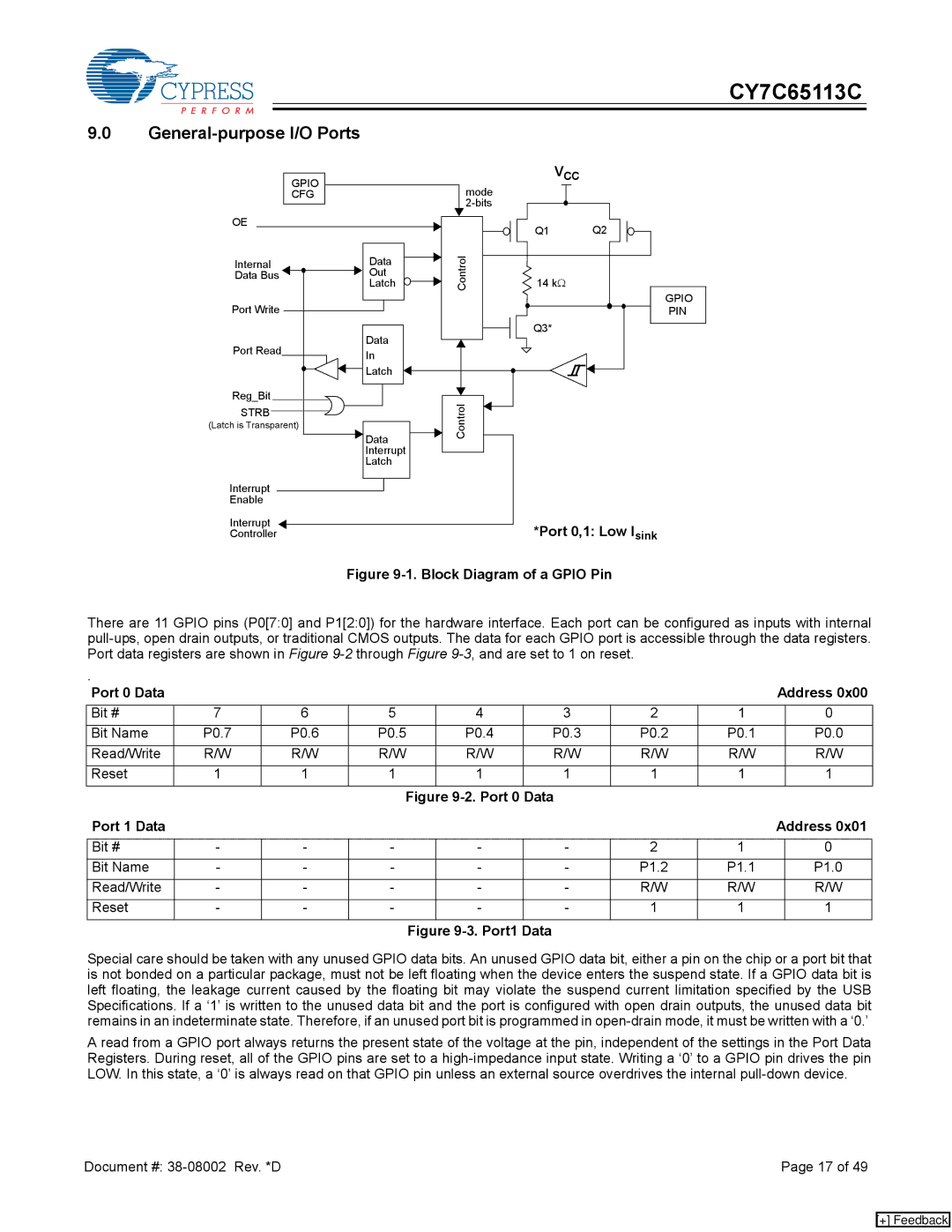
Figure 9-1. Block Diagram of a GPIO Pin
There are 11 GPIO pins (P0[7:0] and P1[2:0]) for the hardware interface. Each port can be configured as inputs with internal
. |
|
|
|
|
|
|
|
|
|
|
Port 0 Data |
|
|
|
|
|
|
| Address 0x00 | ||
Bit # | 7 | 6 | 5 | 4 | 3 | 2 | 1 |
| 0 |
|
Bit Name | P0.7 | P0.6 | P0.5 | P0.4 | P0.3 | P0.2 | P0.1 |
| P0.0 | |
Read/Write | R/W | R/W | R/W | R/W | R/W | R/W | R/W |
| R/W | |
Reset | 1 | 1 | 1 | 1 | 1 | 1 | 1 |
| 1 |
|
|
|
| Figure |
|
|
|
|
| ||
Port 1 Data |
|
|
|
|
|
|
| Address 0x01 | ||
|
|
|
|
|
|
|
|
|
|
|
Bit # | - | - | - | - | - | 2 | 1 |
| 0 |
|
Bit Name | - | - | - | - | - | P1.2 | P1.1 |
| P1.0 |
|
Read/Write | - | - | - | - | - | R/W | R/W |
| R/W |
|
Reset | - | - | - | - | - | 1 | 1 |
| 1 |
|
Figure 9-3. Port1 Data
Special care should be taken with any unused GPIO data bits. An unused GPIO data bit, either a pin on the chip or a port bit that is not bonded on a particular package, must not be left floating when the device enters the suspend state. If a GPIO data bit is left floating, the leakage current caused by the floating bit may violate the suspend current limitation specified by the USB Specifications. If a ‘1’ is written to the unused data bit and the port is configured with open drain outputs, the unused data bit remains in an indeterminate state. Therefore, if an unused port bit is programmed in
A read from a GPIO port always returns the present state of the voltage at the pin, independent of the settings in the Port Data Registers. During reset, all of the GPIO pins are set to a
Document #: | Page 17 of 49 |
[+] Feedback