CY7C65113C
4.2I/O Register Summary
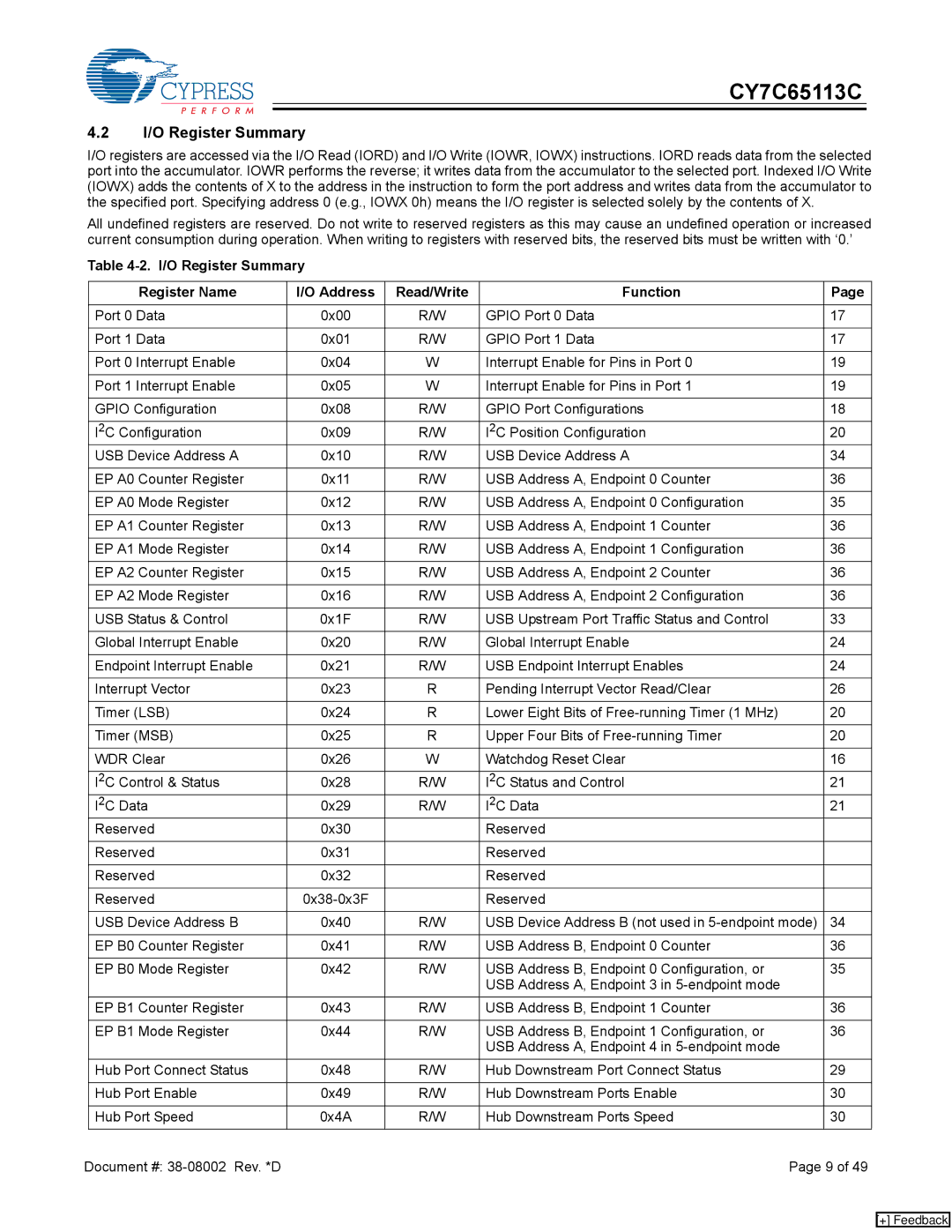
I/O registers are accessed via the I/O Read (IORD) and I/O Write (IOWR, IOWX) instructions. IORD reads data from the selected port into the accumulator. IOWR performs the reverse; it writes data from the accumulator to the selected port. Indexed I/O Write (IOWX) adds the contents of X to the address in the instruction to form the port address and writes data from the accumulator to the specified port. Specifying address 0 (e.g., IOWX 0h) means the I/O register is selected solely by the contents of X.
All undefined registers are reserved. Do not write to reserved registers as this may cause an undefined operation or increased current consumption during operation. When writing to registers with reserved bits, the reserved bits must be written with ‘0.’
Table
| Register Name | I/O Address | Read/Write | Function | Page |
|
|
|
|
|
|
| Port 0 Data | 0x00 | R/W | GPIO Port 0 Data | 17 |
|
|
|
|
|
|
| Port 1 Data | 0x01 | R/W | GPIO Port 1 Data | 17 |
|
|
|
|
|
|
| Port 0 Interrupt Enable | 0x04 | W | Interrupt Enable for Pins in Port 0 | 19 |
|
|
|
|
|
|
| Port 1 Interrupt Enable | 0x05 | W | Interrupt Enable for Pins in Port 1 | 19 |
|
|
|
|
|
|
| GPIO Configuration | 0x08 | R/W | GPIO Port Configurations | 18 |
|
|
|
|
|
|
| I2C Configuration | 0x09 | R/W | I2C Position Configuration | 20 |
| USB Device Address A | 0x10 | R/W | USB Device Address A | 34 |
|
|
|
|
|
|
| EP A0 Counter Register | 0x11 | R/W | USB Address A, Endpoint 0 Counter | 36 |
|
|
|
|
|
|
| EP A0 Mode Register | 0x12 | R/W | USB Address A, Endpoint 0 Configuration | 35 |
|
|
|
|
|
|
| EP A1 Counter Register | 0x13 | R/W | USB Address A, Endpoint 1 Counter | 36 |
|
|
|
|
|
|
| EP A1 Mode Register | 0x14 | R/W | USB Address A, Endpoint 1 Configuration | 36 |
|
|
|
|
|
|
| EP A2 Counter Register | 0x15 | R/W | USB Address A, Endpoint 2 Counter | 36 |
|
|
|
|
|
|
| EP A2 Mode Register | 0x16 | R/W | USB Address A, Endpoint 2 Configuration | 36 |
|
|
|
|
|
|
| USB Status & Control | 0x1F | R/W | USB Upstream Port Traffic Status and Control | 33 |
|
|
|
|
|
|
| Global Interrupt Enable | 0x20 | R/W | Global Interrupt Enable | 24 |
|
|
|
|
|
|
| Endpoint Interrupt Enable | 0x21 | R/W | USB Endpoint Interrupt Enables | 24 |
|
|
|
|
|
|
| Interrupt Vector | 0x23 | R | Pending Interrupt Vector Read/Clear | 26 |
|
|
|
|
|
|
| Timer (LSB) | 0x24 | R | Lower Eight Bits of | 20 |
|
|
|
|
|
|
| Timer (MSB) | 0x25 | R | Upper Four Bits of | 20 |
|
|
|
|
|
|
| WDR Clear | 0x26 | W | Watchdog Reset Clear | 16 |
|
|
|
|
|
|
| I2C Control & Status | 0x28 | R/W | I2C Status and Control | 21 |
| I2C Data | 0x29 | R/W | I2C Data | 21 |
| Reserved | 0x30 |
| Reserved |
|
|
|
|
|
|
|
| Reserved | 0x31 |
| Reserved |
|
|
|
|
|
|
|
| Reserved | 0x32 |
| Reserved |
|
|
|
|
|
|
|
| Reserved |
| Reserved |
| |
|
|
|
|
|
|
| USB Device Address B | 0x40 | R/W | USB Device Address B (not used in | 34 |
|
|
|
|
|
|
| EP B0 Counter Register | 0x41 | R/W | USB Address B, Endpoint 0 Counter | 36 |
|
|
|
|
|
|
| EP B0 Mode Register | 0x42 | R/W | USB Address B, Endpoint 0 Configuration, or | 35 |
|
|
|
| USB Address A, Endpoint 3 in |
|
| EP B1 Counter Register | 0x43 | R/W | USB Address B, Endpoint 1 Counter | 36 |
|
|
|
|
|
|
| EP B1 Mode Register | 0x44 | R/W | USB Address B, Endpoint 1 Configuration, or | 36 |
|
|
|
| USB Address A, Endpoint 4 in |
|
| Hub Port Connect Status | 0x48 | R/W | Hub Downstream Port Connect Status | 29 |
|
|
|
|
|
|
| Hub Port Enable | 0x49 | R/W | Hub Downstream Ports Enable | 30 |
|
|
|
|
|
|
| Hub Port Speed | 0x4A | R/W | Hub Downstream Ports Speed | 30 |
|
|
|
|
|
|
Document #: |
|
| Page 9 of 49 | ||
[+] Feedback