CY7C65113C
Timer LSB |
|
|
|
|
|
|
| Address 0x24 | |
Bit # | 7 | 6 | 5 | 4 | 3 | 2 | 1 |
| 0 |
Bit Name | Timer Bit 7 | TimerBit 6 | Timer Bit 5 | Timer Bit 4 | Timer Bit 3 | Timer Bit 2 | Timer Bit 1 |
| Timer Bit 0 |
Read/Write | R | R | R | R | R | R | R |
| R |
Reset | 0 | 0 | 0 | 0 | 0 | 0 | 0 |
| 0 |
|
|
| Figure |
|
|
|
| ||
Bit [7:0]: Timer lower eight bits. |
|
|
|
|
|
|
| ||
|
|
|
|
|
|
|
|
| |
Timer MSB |
|
|
|
|
|
|
| Address 0x25 | |
Bit # | 7 | 6 | 5 | 4 | 3 | 2 | 1 |
| 0 |
Bit Name | Reserved | Reserved | Reserved | Reserved | Timer Bit 11 | Timer Bit 10 | Timer Bit 9 |
| Timer Bit 8 |
Read/Write | – | – | – | – | R | R | R |
| R |
Reset | 0 | 0 | 0 | 0 | 0 | 0 | 0 |
| 0 |
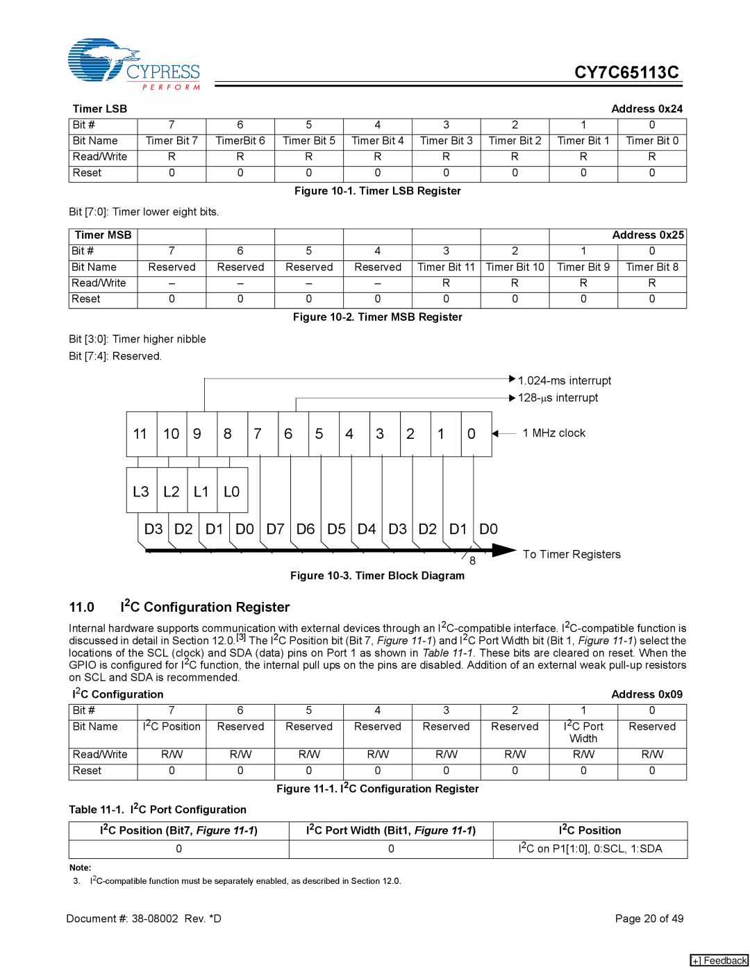
Figure 10-2. Timer MSB Register
Bit [3:0]: Timer higher nibble
Bit [7:4]: Reserved.
![]()
![]()
11
10 9
8
7
6
5
4
3
2
1
0
![]() 1 MHz clock
1 MHz clock
|
|
|
|
|
|
|
|
|
|
|
|
L3 |
| L2 |
| L1 | L0 |
|
| ||||
|
|
|
|
|
|
|
|
|
|
|
|
| D3 |
| D2 |
| D1 | D0 | D7 | ||||
|
|
|
|
|
|
|
|
|
|
|
|
D6 D5 D4 D3 D2 D1 D0
8
Figure 10-3. Timer Block Diagram
![]() To Timer Registers
To Timer Registers
11.0I2C Configuration Register
Internal hardware supports communication with external devices through an
. | I2C Configuration |
|
|
|
|
|
|
|
| Address 0x09 | |||
| Bit # |
| 7 | 6 | 5 | 4 | 3 | 2 | 1 |
| 0 | ||
| Bit Name |
| I2C Position | Reserved | Reserved | Reserved | Reserved | Reserved | I2C Port |
| Reserved | ||
|
|
|
|
|
|
|
|
|
|
| Width |
|
|
|
|
|
|
|
|
|
|
|
|
|
|
|
|
| Read/Write |
| R/W | R/W |
| R/W | R/W | R/W |
| R/W | R/W |
| R/W |
| Reset |
| 0 | 0 | 0 | 0 | 0 | 0 | 0 |
| 0 | ||
|
|
|
|
| Figure | 2C Configuration Register |
|
|
|
|
| ||
Table | I2C Port Configuration |
|
|
|
|
|
|
|
|
| |||
| I2C Position (Bit7, Figure |
| I2C Port Width (Bit1, Figure |
|
| I2C Position | |||||||
|
| 0 |
|
|
| 0 |
|
| I2C on P1[1:0], 0:SCL, 1:SDA | ||||
Note:
3.
Document #: | Page 20 of 49 |
[+] Feedback