Freescale Semiconductor, Inc
MPC860T Rev. D Fast Ethernet Controller
Motorola Literature Distribution Centers
Contents
Parallel I/O Ports
Contents
Paragraph Title Number
Title Number
Illustrations
Viii MPC860T Rev. D Fast Ethernet Controller Supplement
Tables
Number
Overview
Document Revision History
Lists signiÞcant changes between revisions of this document
Document Revision History
Comparison with the MPC860
Features
1 MPC860TBlock Diagram
Fast Ethernet Controller
Embedded PowerPC Processor Core
System Interface Unit SIU
SIU Interrupt ConÞguration
Glueless System Design
Inc
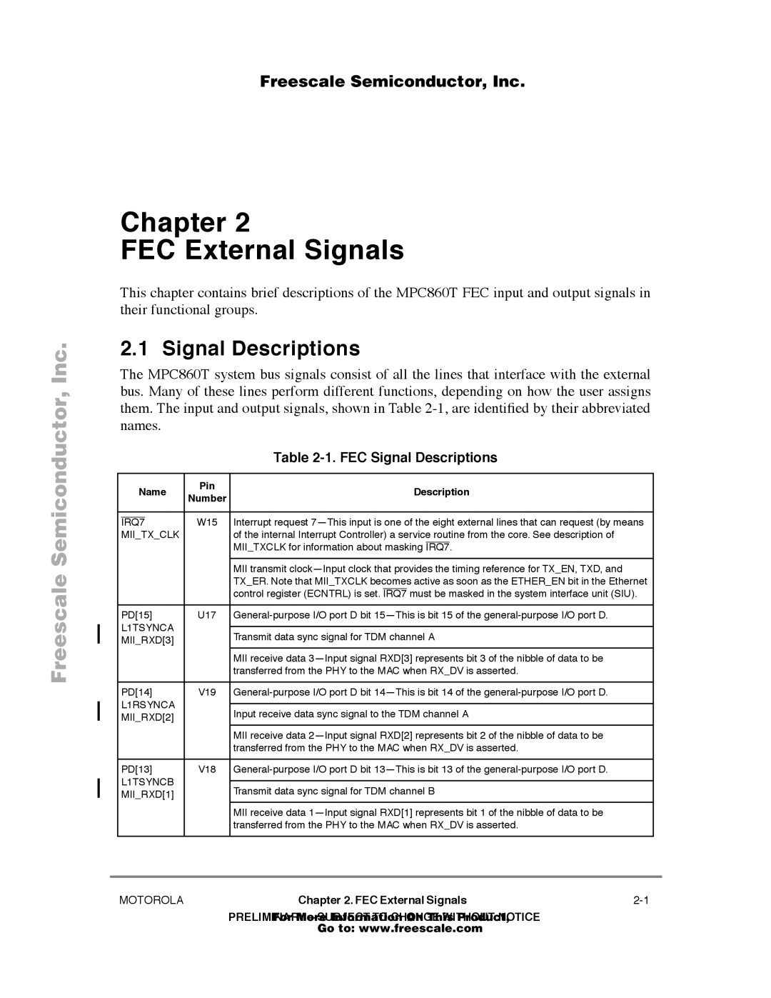
Name Pin Description
Signal Descriptions
FEC Signal Descriptions
Miimdc
L1RSYNCB
RXD3
Miitxer
MIITXD2
REJECT3
REJECT4
MIITXD1
Freescale Semiconductor, Inc
Signal Description FEC Signal Name
MII Signals
Transceiver Connection
This chapter discusses the operation of the FEC
FEC Frame Transmission
Serial Mode Connections to the External Transceiver
TXD0
RXD0
FEC Frame Reception
Ethernet Address Recognition
FEC Command Set
CAM Interface
Rcntrlprom =
Hash Table Algorithm
Collision Handling
Inter-Packet Gap Time
Transmission Errors
Ethernet Error-Handling Procedure
Reception Errors
Internal and External Loopback
Reception Errors
Port D Pin Functions
Chapter Parallel I/O Ports
Signal Function
Enabling MII Mode
Port D Registers
Shows the port D pin assignments
CLK
Sdma Registers
Sdcr Field Descriptions
Describes Sdcr Þelds
FRZ Faid RAID
Bits
Brießy describes each enter in the FEC parameter RAM
Parameter RAM
FEC Parameter RAM Memory Map
Address Name Description Section
RAM Perfect Match Address Low Register Addrlow
RAM Hash Table High Hashtablehigh
RAM Perfect Match Address High Addrhigh
Describes the Addrlow Þelds
Describes the Addrhigh Þelds
Describes Hashtablehigh Þelds
RAM Hash Table Low Hashtablelow
Hashtablehigh Field Descriptions
Hashhigh
Beginning of TxBD Ring Xdesstart
Beginning of RxBD Ring Rdesstart
Describes Hashtablelow Þelds
Describes Rdesstart Þelds
Xdesstart Field Descriptions
Receive Buffer Size Register Rbuffsize
Describes Xdesstart Þelds
Ethernet Control Register Ecntrl
Spare Fecpin Etheren Reset MUX
Describes Rbuffsize Þelds
Rbuffsize Field Descriptions
Describes Ecntrl Þelds
Interrupt Event IEVENT/Interrupt Mask Register Imask
Ecntrl Field Descriptions
Fecpinmux
Rfint to notify at the end of frame
Ethernet Interrupt Vector Register Ivec
10. IEVENT/IMASK Field Descriptions
Hberr
11 describes Ivec Þelds
RxBD Active Register Rdesactive
11. Ivec Field Descriptions
Ilevel
12. Rdesactive Field Descriptions
TxBD Active Register Xdesactive
12 describes Rdesactive Þelds
13. Xdesactive Field Descriptions
MII Management Frame Register Miidata
13 describes Xdesactive Þelds
14. Miidata Field Descriptions
14 describes Miidata Þelds
15 describes Miispeed Þelds
MII Speed Control Register Miispeed
15. Miispeed Field Descriptions
Dispreamble Miispeed
17 describes Rbound Þelds
Fifo Receive Bound Register Rbound
16. Programming Examples for Miispeed Register
17. Rbound Field Descriptions
Transmit Watermark Register Xwmrk
Fifo Receive Start Register Rfstart
18 describes Rñfstart Þelds
18. Rfstart Field Descriptions
19. Xwmrk Field Descriptions
Fifo Transmit Start Register Xfstart
19 bit Þeld descriptions for Xwmrk
20 describes Xfstart Þelds
DMA Function Code Register Funcode
20. Xfstart Field Descriptions
DATABO0 DATABO1 DESCBO0 DESCBO1 FC1 FC2 FC3
21 describes Funcode Þelds
Receive Control Register Rcntrl
21. Funcode Field Descriptions
Descbo
22 describes Rcntrl Þelds
Receive Hash Register Rhash
22. Rcntrl Field Descriptions
Bcrej
22 describes Rhash Þelds
Transmit Control Register Xcntrl
24 describes Xcntrl Þelds
23. Rhash Field Descriptions
Initialization Sequence
User Initialization before Setting Ecntrletheren
Hardware Initialization
25. Hardware Initialization
Descriptor Controller Initialization
27. User Initialization before Setting Ecntrletheren
User Initialization after Asserting Ecntrletheren
Step Description
Buffer Descriptors BDs
27. User Initialization after Setting Ecntrletheren
Ethernet Receive Buffer Descriptor RxBD
Step
27. Receive Buffer Descriptor RxBD Field Description
RxBD format is shown in Table
RO1 RO2 Data Length
RO1
29 describes TxBD Þelds
Ethernet Transmit Buffer Descriptor TxBD
29. Transmit Buffer Descriptor TxBD Field Descriptions
TO1 TO2 DEF CSL
Data
Xcntrlhbc =
Freescale Semiconductor, Inc
AC Electrical Characteristics
DC Electrical Characteristics
MII Receive Signal Timing RXD30, RXDV, RXER, Rxclk
Electrical SpeciÞcations
MII Receive Signal Timing
MII Transmit Signal Timing TXD30, TXEN, TXER, Txclk
MII Transmit Signal Timing
Num Characteristic Min Max Unit
MII Async Inputs Signal Timing
MII Async Inputs Signal Timing CRS, COL
Txen Txer
CRS, COL
MII Serial Management Channel Timing
Shows the MII serial management channel timing diagram
MPC860T Pin Assignments
Following pins are marked as spare on
Freescale Semiconductor, Inc
Freescale Semiconductor, Inc
For More Information On This Product