Package Information |
|
|
|
| |
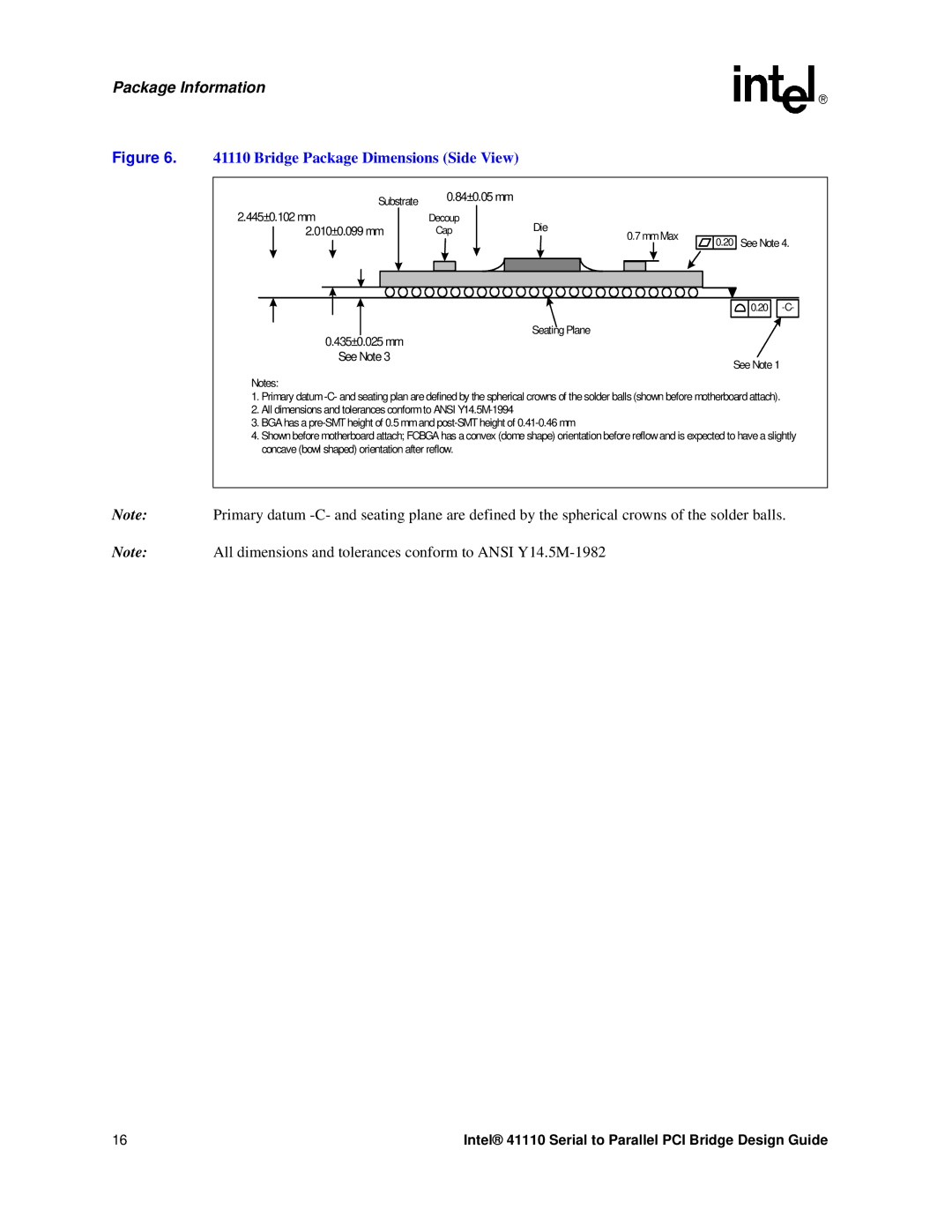
Figure 6. | 41110 Bridge Package Dimensions (Side View) |
|
|
| |
| Substrate | 0.84±0.05 mm |
|
|
|
|
|
|
|
| |
| 2.445±0.102 mm | Decoup | Die |
|
|
| 2.010±0.099 mm | Cap | 0.7 mmMax | 0.20 See Note 4. | |
|
|
|
| ||
|
|
|
|
| |
|
|
|
|
| 0.20 |
| 0.435±0.025 mm |
| Seating Plane |
|
|
|
|
|
|
| |
| See Note 3 |
|
|
| See Note 1 |
|
|
|
|
| |
Notes:
1.Primary
2.All dimensions and tolerances conformto ANSI
3.BGAhas a
4.Shown before motherboard attach; FCBGA has a convex (dome shape) orientation before reflowand is expected to have a slightly concave (bowl shaped) orientation after reflow.
Note: Primary datum
Note: All dimensions and tolerances conform to ANSI
16 | Intel® 41110 Serial to Parallel PCI Bridge Design Guide |