Board Layout Guidelines | 7 |
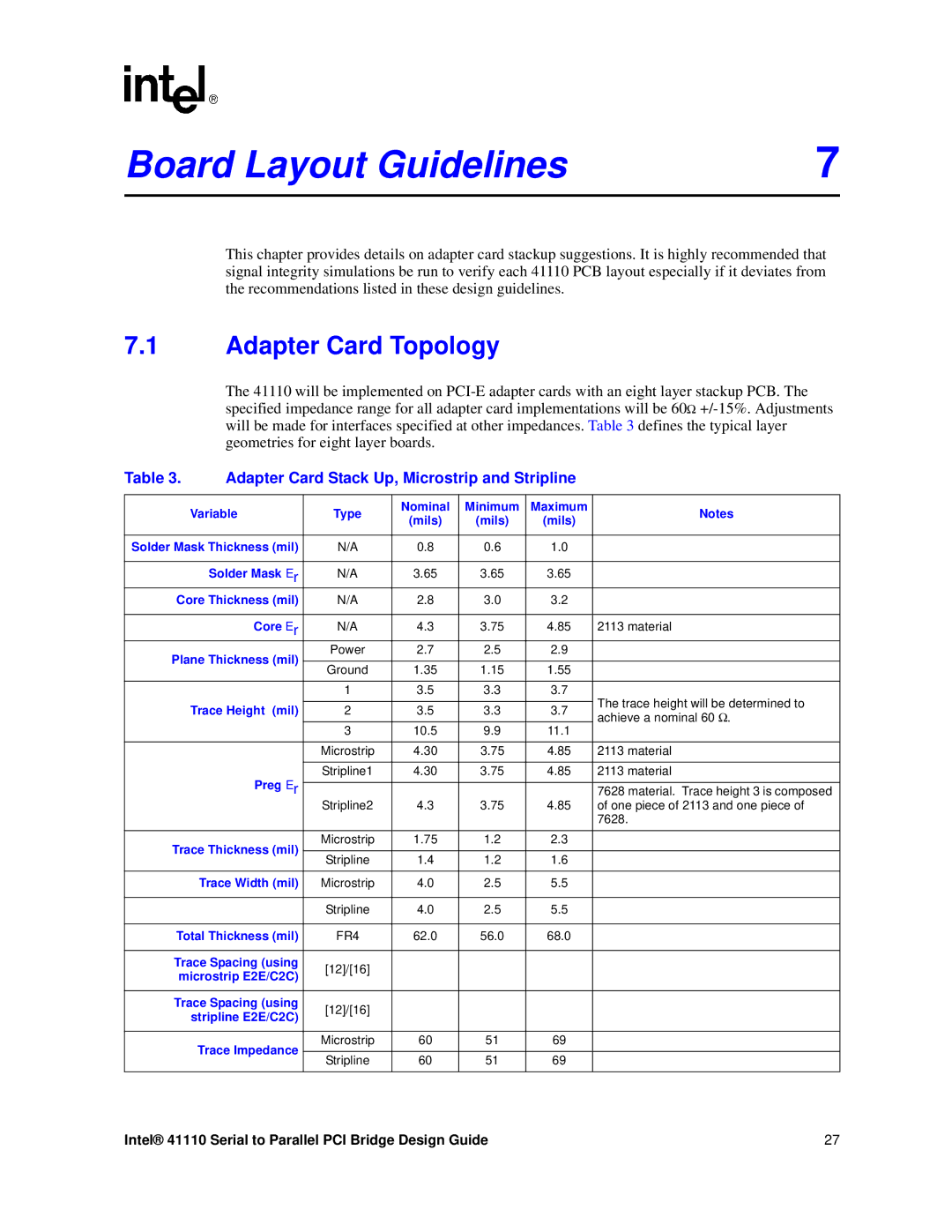
This chapter provides details on adapter card stackup suggestions. It is highly recommended that signal integrity simulations be run to verify each 41110 PCB layout especially if it deviates from the recommendations listed in these design guidelines.
7.1Adapter Card Topology
The 41110 will be implemented on
Table 3. | Adapter Card Stack Up, Microstrip and Stripline |
| ||||
|
|
|
|
|
|
|
| Variable | Type | Nominal | Minimum | Maximum | Notes |
| (mils) | (mils) | (mils) | |||
|
|
|
| |||
|
|
|
|
|
| |
Solder Mask Thickness (mil) | N/A | 0.8 | 0.6 | 1.0 |
| |
|
|
|
|
|
|
|
| Solder Mask Er | N/A | 3.65 | 3.65 | 3.65 |
|
Core Thickness (mil) | N/A | 2.8 | 3.0 | 3.2 |
| |
|
|
|
|
|
|
|
| Core Er | N/A | 4.3 | 3.75 | 4.85 | 2113 material |
Plane Thickness (mil) | Power | 2.7 | 2.5 | 2.9 |
| |
|
|
|
|
| ||
Ground | 1.35 | 1.15 | 1.55 |
| ||
|
|
| ||||
|
|
|
|
|
|
|
|
| 1 | 3.5 | 3.3 | 3.7 | The trace height will be determined to |
| Trace Height (mil) |
|
|
|
| |
| 2 | 3.5 | 3.3 | 3.7 | ||
| achieve a nominal 60 Ω. | |||||
|
|
|
|
|
| |
|
| 3 | 10.5 | 9.9 | 11.1 |
|
|
|
|
|
|
|
|
|
| Microstrip | 4.30 | 3.75 | 4.85 | 2113 material |
|
|
|
|
|
|
|
| Preg Er | Stripline1 | 4.30 | 3.75 | 4.85 | 2113 material |
|
|
|
|
|
| |
|
|
|
|
| 7628 material. Trace height 3 is composed | |
|
| Stripline2 | 4.3 | 3.75 | 4.85 | of one piece of 2113 and one piece of |
|
|
|
|
|
| 7628. |
|
|
|
|
|
|
|
Trace Thickness (mil) | Microstrip | 1.75 | 1.2 | 2.3 |
| |
|
|
|
|
| ||
Stripline | 1.4 | 1.2 | 1.6 |
| ||
|
|
| ||||
|
|
|
|
|
|
|
| Trace Width (mil) | Microstrip | 4.0 | 2.5 | 5.5 |
|
|
|
|
|
|
|
|
|
| Stripline | 4.0 | 2.5 | 5.5 |
|
|
|
|
|
|
| |
Total Thickness (mil) | FR4 | 62.0 | 56.0 | 68.0 |
| |
|
|
|
|
|
| |
Trace Spacing (using | [12]/[16] |
|
|
|
| |
microstrip E2E/C2C) |
|
|
|
| ||
|
|
|
|
| ||
|
|
|
|
|
| |
Trace Spacing (using | [12]/[16] |
|
|
|
| |
| stripline E2E/C2C) |
|
|
|
| |
|
|
|
|
|
| |
|
|
|
|
|
|
|
| Trace Impedance | Microstrip | 60 | 51 | 69 |
|
|
|
|
|
|
| |
| Stripline | 60 | 51 | 69 |
| |
|
|
| ||||
|
|
|
|
|
|
|
Intel® 41110 Serial to Parallel PCI Bridge Design Guide | 27 |