41110 Customer Reference Boards
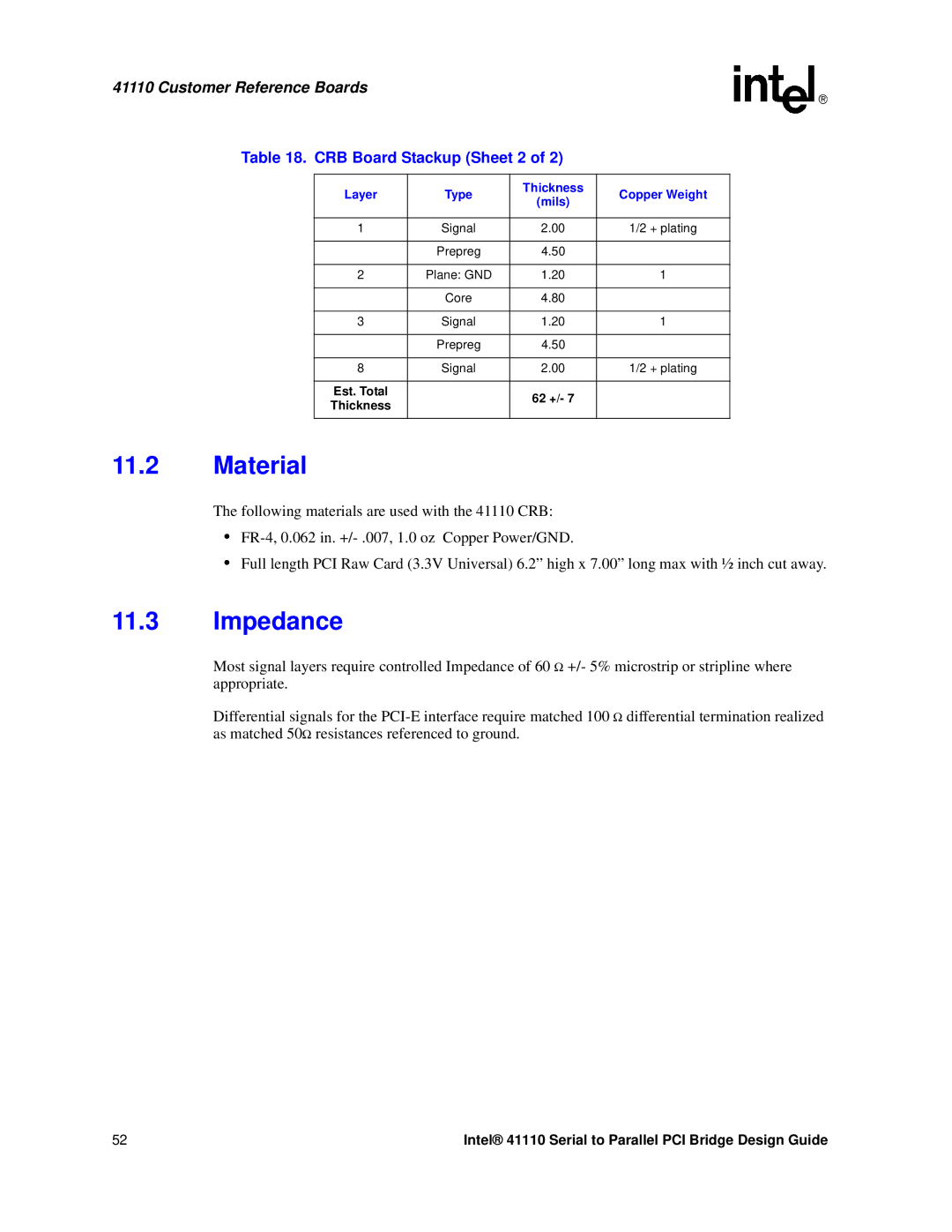
Table 18. CRB Board Stackup (Sheet 2 of 2)
Layer | Type | Thickness | Copper Weight | |
(mils) | ||||
|
|
| ||
|
|
|
| |
1 | Signal | 2.00 | 1/2 + plating | |
|
|
|
| |
| Prepreg | 4.50 |
| |
|
|
|
| |
2 | Plane: GND | 1.20 | 1 | |
|
|
|
| |
| Core | 4.80 |
| |
|
|
|
| |
3 | Signal | 1.20 | 1 | |
|
|
|
| |
| Prepreg | 4.50 |
| |
|
|
|
| |
8 | Signal | 2.00 | 1/2 + plating | |
|
|
|
| |
Est. Total |
| 62 +/- 7 |
| |
Thickness |
|
| ||
|
|
| ||
|
|
|
|
11.2Material
The following materials are used with the 41110 CRB:
•
•Full length PCI Raw Card (3.3V Universal) 6.2” high x 7.00” long max with ½ inch cut away.
11.3Impedance
Most signal layers require controlled Impedance of 60 Ω +/- 5% microstrip or stripline where appropriate.
Differential signals for the
52 | Intel® 41110 Serial to Parallel PCI Bridge Design Guide |
