41110 Customer Reference Boards 11
This chapter describes the 41110 Customer Reference Board (CRB).
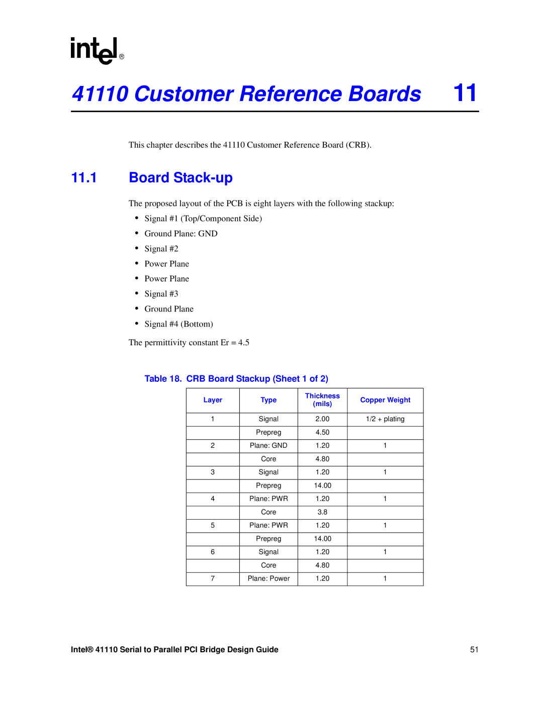
11.1Board Stack-up
The proposed layout of the PCB is eight layers with the following stackup:
•Signal #1 (Top/Component Side)
•Ground Plane: GND
•Signal #2
•Power Plane
•Power Plane
•Signal #3
•Ground Plane
•Signal #4 (Bottom)
The permittivity constant Er = 4.5
Table 18. CRB Board Stackup (Sheet 1 of 2)
Layer | Type | Thickness | Copper Weight | |
(mils) | ||||
|
|
| ||
|
|
|
| |
1 | Signal | 2.00 | 1/2 + plating | |
|
|
|
| |
| Prepreg | 4.50 |
| |
|
|
|
| |
2 | Plane: GND | 1.20 | 1 | |
|
|
|
| |
| Core | 4.80 |
| |
|
|
|
| |
3 | Signal | 1.20 | 1 | |
|
|
|
| |
| Prepreg | 14.00 |
| |
|
|
|
| |
4 | Plane: PWR | 1.20 | 1 | |
|
|
|
| |
| Core | 3.8 |
| |
|
|
|
| |
5 | Plane: PWR | 1.20 | 1 | |
|
|
|
| |
| Prepreg | 14.00 |
| |
|
|
|
| |
6 | Signal | 1.20 | 1 | |
|
|
|
| |
| Core | 4.80 |
| |
|
|
|
| |
7 | Plane: Power | 1.20 | 1 | |
|
|
|
|
Intel® 41110 Serial to Parallel PCI Bridge Design Guide | 51 |