About This Document
Table 1. Terminology and Definitions (Sheet 2 of 2)
Term |
|
|
|
|
|
|
| Definition | |||||
|
|
|
|
|
|
|
|
|
|
|
|
|
|
|
|
|
|
|
| Layer 1: copper | Printed circuit board. | ||||||
|
|
|
|
|
| Example manufacturing process consists of | |||||||
|
|
|
|
|
| ||||||||
|
|
|
|
|
| Prepreg | the following steps: | ||||||
|
|
|
|
|
| Layer 2: GND | |||||||
|
|
|
|
|
| ||||||||
|
|
|
|
|
|
| • Consists of alternating layers of core and | ||||||
|
|
|
|
|
|
|
|
|
| ||||
|
|
|
|
|
| Core |
| prepreg stacked | |||||
PCB |
|
|
|
|
| Layer 3: VCC15 |
| • The finished PCB is heated and cured. | |||||
|
|
|
|
|
| • The via holes are drilled | |||||||
|
|
|
|
|
| Prepreg |
| ||||||
|
|
|
|
|
| Layer 4: copper |
| • Plating covers holes and outer surfaces | |||||
|
|
|
|
|
| ||||||||
|
|
|
|
|
|
|
|
|
| • Etching removes unwanted copper | |||
|
|
| Example of a |
| • Board is tinned, coated with solder mask | ||||||||
|
|
|
| and silk screened | |||||||||
|
|
|
|
|
|
|
|
|
|
|
|
|
|
SSTL_2 | Series Stub Terminated Logic for 2.5 V |
|
|
|
|
| |||||||
|
|
|
|
|
|
|
|
|
|
|
|
| |
JEDEC | Provides standards for the semiconductor industry. | ||||||||||||
|
|
|
|
|
|
|
|
|
|
|
|
| |
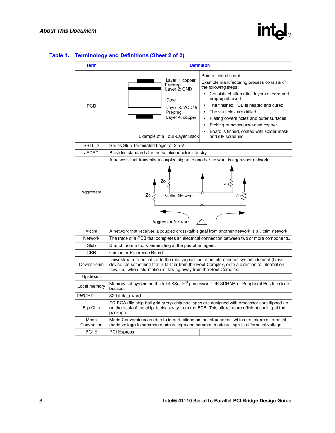
| A network that transmits a coupled signal to another network is aggressor network. | ||||||||||||
|
|
|
|
|
|
|
|
|
|
|
| ||
|
|
|
|
| Zo |
|
|
|
|
|
|
| |
Aggressor |
|
| Zo |
|
|
| Zo |
|
| ||||
|
|
|
|
|
|
|
|
|
| ||||
|
|
|
|
|
|
|
| ||||||
|
|
|
|
|
|
|
|
|
|
|
| ||
|
|
|
|
|
|
|
|
| Zo | ||||
|
|
|
|
| Victim Network |
|
| ||||||
|
|
|
|
|
|
|
|
|
|
| |||
|
|
|
|
|
|
|
|
|
|
| |||
|
|
|
| Aggressor Network |
|
|
|
|
| ||||
|
|
|
|
|
|
|
|
| |||||
|
|
|
|
|
|
|
|
|
|
|
|
| |
Victim | A network that receives a coupled | ||||||||||||
|
|
|
|
|
|
|
|
|
|
|
|
| |
Network | The trace of a PCB that completes an electrical connection between two or more components. | ||||||||||||
|
|
|
|
|
|
|
|
|
|
|
|
| |
Stub | Branch from a trunk terminating at the pad of an agent. | ||||||||||||
|
|
|
|
|
|
|
|
|
|
|
|
|
|
CRB | Customer Reference Board |
|
|
|
|
| |||||||
|
|
|
|
|
|
|
|
|
|
|
|
| |
| Downstream refers either to the relative position of an interconnect/system element (Link/ | ||||||||||||
Downstream | device) as something that is farther from the Root Complex, or to a direction of information | ||||||||||||
| flow, i.e., when information is flowing away from the Root Complex. | ||||||||||||
|
|
|
|
|
|
|
|
|
|
|
|
|
|
Upstream |
|
|
|
|
|
|
|
|
|
|
|
|
|
|
|
|
|
|
|
|
|
|
|
|
|
| |
Local memory | Memory subsystem on the Intel XScale® processor DDR SDRAM or Peripheral Bus Interface | ||||||||||||
busses. |
|
|
|
|
|
|
|
|
|
| |||
DWORD |
|
|
|
|
|
|
|
|
|
|
| ||
|
|
|
|
|
|
|
|
|
|
|
|
| |
| |||||||||||||
Flip Chip | on the back of the chip, facing away from the PCB. This allows more efficient cooling of the | ||||||||||||
| package. |
|
|
|
|
|
|
|
|
|
| ||
|
|
|
|
|
|
|
|
|
|
|
|
| |
Mode | Mode Conversions are due to imperfections on the interconnect which transform differential | ||||||||||||
Conversion | mode voltage to common mode voltage and common mode voltage to differential voltage. | ||||||||||||
|
|
|
|
|
|
|
|
|
| ||||
|
|
|
|
|
|
|
|
|
|
|
|
|
|
8 | Intel® 41110 Serial to Parallel PCI Bridge Design Guide |
