iv IntelĀ® 41110 Serial to Parallel PCI Bridge Design Guide
Contents
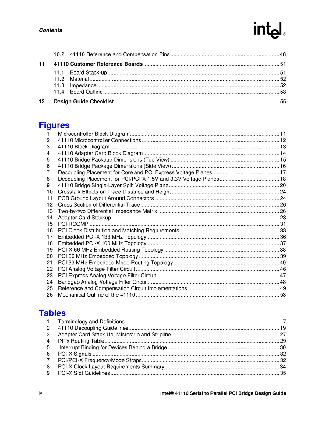
10.2 41110 Reference and Compensation Pins ......................................................................... 48
11 41110 Customer Reference Boards .......................................................... .................................51
11.1 Board Stack-up.............................. ....... ...... ....... ...... ...... ....... ...... ....... ...... ....... ....................51
11.2 Material............................. .................................................................................................. 52
11.3 Impedance........................ .................................................................................................. 52
11.4 Board Outline........................................................... ...... ....... ...... ........................................53
12 Design Guide Checklist ......................... ..................................................................................... 55
Figures
1 Microcontroller Block Diagram............................................................................................. .......11
2 41110 Microcontroller Connections.............. .............................................................................. 12
3 41110 Block Diagram......... ........................................................................................................ 13
4 41110 Adapter Card Block Diagram.......................................................... .................................14
5 41110 Bridge Package Dimensions (Top View) ......................................................................... 15
6 41110 Bridge Package Dimensions (Side View) ........................................................................ 16
7 Decoupling Placement for Core and PCI Express Voltage Planes ................. ...........................17
8 Decoupling Placement for PCI/PCI-X 1.5V and 3.3V Voltage Planes ........................................ 18
9 41110 Bridge Single-Layer Split Voltage Plane...................................................... ....................20
10 Crosstalk Effects on Trace Distance and Height ........................................................................ 24
11 PCB Ground Layout Around Connectors ............................................................... ....................24
12 Cross Section of Differential Trace..................................................... ........................................ 26
13 Two-by-two Differential Impedance Matrix ................................................................................. 26
14 Adapter Card Stackup.............. ....... ...... ....... ...... ....... ...... ...... ....... ...... ....... ...... ....... ....................28
15 PCI RCOMP....................... ........................................................................................................ 31
16 PCI Clock Distribution and Matching Requirements..................................................... ..............33
17 Embedded PCI-X 133 MHz Topology ....................... ................................................................. 36
18 Embedded PCI-X 100 MHz Topology ....................... ................................................................. 37
19 PCI-X 66 MHz Embedded Routing Topology ............................................................................ .38
20 PCI 66 MHz Embedded Topology ....................................................................................... .......39
21 PCI 33 MHz Embedded Mode Routing Topology.................. ..................................................... 40
22 PCI Analog Voltage Filter Circuit.................. .............................................................................. 46
23 PCI Express Analog Voltage Filter Circuit.......... ........................................................................ 47
24 Bandgap Analog Voltage Filter Circuit.................................................................... ....................48
25 Reference and Compensation Circuit Implementations ............................................................. 49
26 Mechanical Outline of the 41110.................. .............................................................................. 53
Tables
1 Terminology and Definitions......................... ................................................................................ 7
2 41110 Decoupling Guidelines.......................................................................... ...........................19
3 Adapter Card Stack Up, Microstrip and Stripline ........................................................................ 27
4 INTx Routing Table....................................................................................................... ..............29
5 Interrupt Binding for Devices Behind a Bridge............................................................. ..............30
6 PCI-X Signals..................... ........................................................................................................ 32
7 PCI/PCI-X Frequency/Mode Straps.............................................................................. ..............32
8 PCI-X Clock Layout Requirements Summary .............................................................. ..............34
9 PCI-X Slot Guidelines................................................................... .............................................. 35