Design Guide Checklist
Table 24. Power and Ground Signals
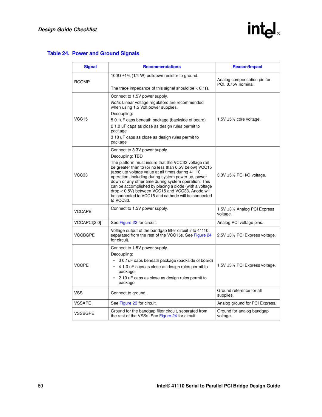
Signal | Recommendations | Reason/Impact | |
|
|
| |
| 100Ω ±1% (1/4 W) pulldown resistor to ground. | Analog compensation pin for | |
RCOMP |
| ||
| PCI. 0.75V nominal. | ||
| The trace impedance of this signal should be < 0.1Ω. | ||
|
| ||
|
|
| |
| Connect to 1.5V power supply. |
| |
| Note: Linear voltage regulators are recommended |
| |
| when using 1.5 Volt power supplies. |
| |
| Decoupling: |
| |
VCC15 | 5 0.1uF caps beneath package (backside of board) | 1.5V ±5% core voltage. | |
| 2 1.0 uF caps as close as design rules permit to |
| |
| package |
| |
| 3 10 uF caps as close as design rules permit to |
| |
| package |
| |
|
|
| |
| Connect to 3.3V power supply. |
| |
| Decoupling: TBD |
| |
| The platform must insure that the VCC33 voltage rail |
| |
| be greater than to (or no less than 0.5V below) VCC15 |
| |
VCC33 | (absolute voltage value at all times during 41110 | 3.3V ±5% PCI I/O voltage. | |
operation, including during system power up, power | |||
| down or any other time during system operation. This |
| |
| can be accomplished by placing a diode (with a voltage |
| |
| drop < 0.5V) between VCC15 and VCC33. Anode will |
| |
| be connected to VCC15 and cathode will be connected |
| |
| to VCC33. |
| |
|
|
| |
VCCAPE | Connect to 1.5V power supply. | 1.5V ±3% Analog PCI Express | |
| voltage. | ||
|
| ||
|
|
| |
VCCAPCI[2:0] | See Figure 22 for circuit. | Analog PCI voltage pins. | |
|
|
| |
| Voltage output of the bandgap filter circuit into 41110, |
| |
VCCBGPE | separated from the rest of the VCC15s. See Figure 24 | 2.5V ±3% PCI Express voltage. | |
| for circuit. |
| |
|
|
| |
| Connect to 1.5V power supply. |
| |
| Decoupling: |
| |
VCCPE | • 3 0.1uF caps beneath package (backside of board) | 1.5V ±3% PCI Express voltage. | |
• 4 1.0 uF caps as close as design rules permit to | |||
| package |
| |
| • 2 10 uF caps as close as design rules permit to |
| |
| package |
| |
|
|
| |
VSS | Connect to ground. | Ground reference for all | |
supplies. | |||
|
| ||
|
|
| |
VSSAPE | See Figure 23 for circuit. | Analog ground for PCI Express. | |
|
|
| |
VSSBGPE | Ground for the bandgap filter circuit, separated from | Ground for analog bandgap | |
the rest of the VSSs. See Figure 24 for circuit. | voltage. | ||
| |||
|
|
|
60 | Intel® 41110 Serial to Parallel PCI Bridge Design Guide |