|
| |
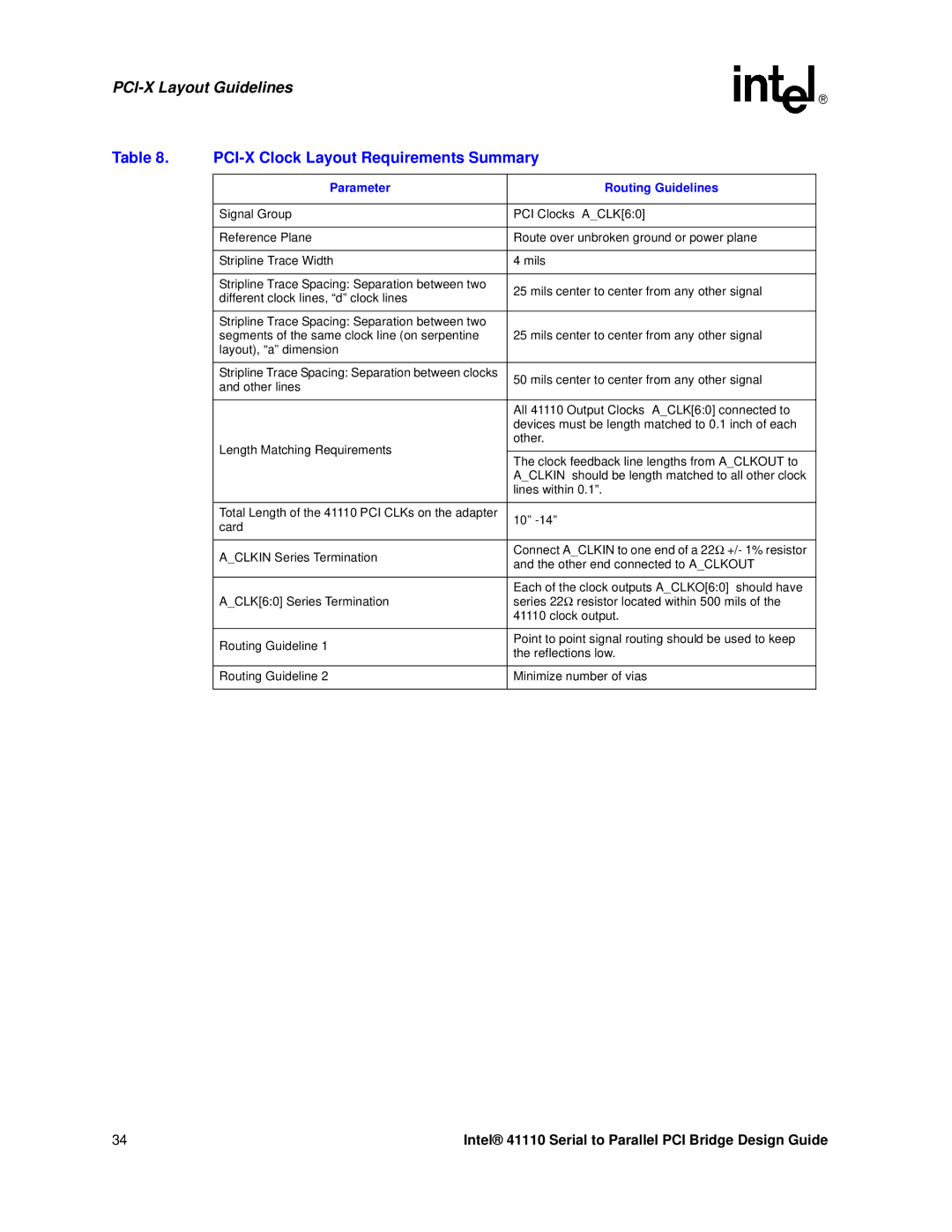
Table 8. |
| |
|
|
|
| Parameter | Routing Guidelines |
|
|
|
| Signal Group | PCI Clocks A_CLK[6:0] |
|
|
|
| Reference Plane | Route over unbroken ground or power plane |
|
|
|
| Stripline Trace Width | 4 mils |
|
|
|
| Stripline Trace Spacing: Separation between two | 25 mils center to center from any other signal |
| different clock lines, “d” clock lines | |
|
| |
|
|
|
| Stripline Trace Spacing: Separation between two |
|
| segments of the same clock line (on serpentine | 25 mils center to center from any other signal |
| layout), “a” dimension |
|
|
|
|
| Stripline Trace Spacing: Separation between clocks | 50 mils center to center from any other signal |
| and other lines | |
|
| |
|
|
|
|
| All 41110 Output Clocks A_CLK[6:0] connected to |
|
| devices must be length matched to 0.1 inch of each |
| Length Matching Requirements | other. |
|
| |
| The clock feedback line lengths from A_CLKOUT to | |
|
| |
|
| A_CLKIN should be length matched to all other clock |
|
| lines within 0.1”. |
|
|
|
| Total Length of the 41110 PCI CLKs on the adapter | 10” |
| card | |
|
| |
|
|
|
| A_CLKIN Series Termination | Connect A_CLKIN to one end of a 22Ω +/- 1% resistor |
| and the other end connected to A_CLKOUT | |
|
| |
|
|
|
|
| Each of the clock outputs A_CLKO[6:0] should have |
| A_CLK[6:0] Series Termination | series 22Ω resistor located within 500 mils of the |
|
| 41110 clock output. |
|
|
|
| Routing Guideline 1 | Point to point signal routing should be used to keep |
| the reflections low. | |
|
| |
|
|
|
| Routing Guideline 2 | Minimize number of vias |
|
|
|
34 | Intel® 41110 Serial to Parallel PCI Bridge Design Guide |