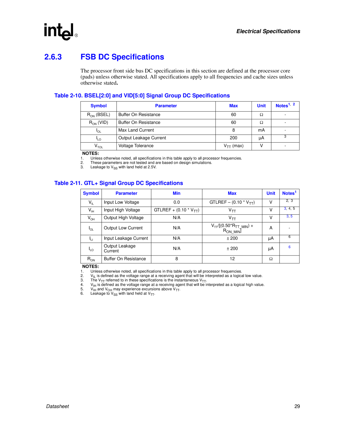
830 specifications
The Intel 830 chipset, introduced in the early 2000s, marked a significant evolution in Intel's chipset architecture for desktop and mobile computing. Known for its support of the Pentium 4 processors, the 830 chipset was tailored for both performance and stability, making it an appealing choice for OEMs and enthusiasts alike.One of the standout features of the Intel 830 chipset is its support for DDR SDRAM, providing a much-needed boost in memory bandwidth compared to its predecessors. With dual-channel memory support, the chipset could utilize two memory modules simultaneously, which effectively doubled the data transfer rate and enhanced overall system performance. This made the Intel 830 particularly beneficial for applications requiring high memory throughput, such as multimedia processing and gaming.
Another important characteristic of the Intel 830 was its integrated graphics support, featuring Intel's Extreme Graphics technology. This integration allowed for decent graphics performance without the need for a dedicated GPU, making it suitable for budget systems and everyday computing tasks. However, for power users and gaming enthusiasts, the option to incorporate a discrete graphics card remained available through the provided PCI Express x16 slot.
The Intel 830 chipset also boasted advanced I/O capabilities, including support for USB 2.0, which provided faster data transfer rates compared to USB 1.1, and enhanced IDE interfaces for connecting hard drives and optical devices. With its Hyper-Threading technology support, the chipset allowed for improved multitasking efficiency, enabling a single processor to execute multiple threads simultaneously, a feature that was particularly beneficial in server environments and complex computing tasks.
In terms of connectivity, the Intel 830 supported multiple bus interfaces, including PCI Express and AGP, thereby enabling users to expand their systems with various add-on cards. This flexibility contributed to the chipset's longevity in the marketplace, as it catered to a wide range of user needs from light computing to intensive gaming and content creation.
In summary, the Intel 830 chipset combined enhanced memory capabilities, integrated graphics performance, robust I/O features, and flexible expansion options, making it a versatile choice for various computing environments during its time. It played a key role in shaping the landscape of early 2000s computing, paving the way for future advancements in chipset technology. Its legacy continues to influence modern computing architectures, illustrating the lasting impact of Intel’s innovative design principles.
